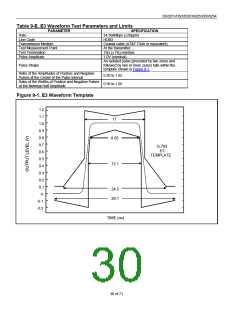
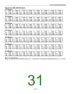
DS3251/DS3252/DS3253/DS3254
11. DIAGNOSTICS
11.1 PRBS Generator and Detector
Each LIU has built-in pseudorandom bit sequence (PRBS) generator and detector circuitry for physical layer
testing. The device generates and detects unframed 215 - 1 (DS3 or STS-1) or 223 - 1 PRBS, according to the ITU
O.151 specification. To transmit a PRBS pattern, pull the TDSA and TDSB pins high (hardware mode) or set
configuration bits TDSA and TDSB in the GCR register (CPU bus mode). As Table 6-G shows, the PRBS
generator automatically generates 215 - 1 for DS3 and STS-1 modes and 223 - 1 for E3 mode.
The PRBS detector, which is always enabled (Table 6-H), reports its status through the PRBS output pin (hardware
and CPU bus modes) or through the PRBS and PBER status bits (CPU bus mode). When the PRBS detector is out
of synchronization, the PRBS pin is forced high. When the detector syncs to an incoming PRBS pattern, the PRBS
pin is driven low, then pulses high, synchronous with RCLK, for each bit error detected. See Figure 11-1 and Figure
11-2 for details. In CPU bus mode, the PRBS status bit is set to one when the detector is out of synchronization
and set to zero when the detector syncs to an incoming PRBS pattern. A change of state of the PRBS bit sets the
PRBSL bit in the SRL register and can also cause an interrupt on the INT pin if the PRBSIE bit in the SRIE register
is set to one. A pattern bit error set the PBERL bit in the SRL register and can also cause an interrupt if the
PBERIE bit in the SRIE register is set to one.
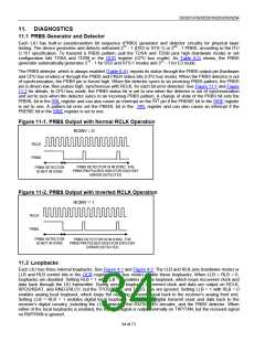
Figure 11-1. PRBS Output with Normal RCLK Operation
RCINV = 0
RCLK
PRBS
PRBS DETECTOR IS IN SYNC; THE
PRBS PIN PULSES HIGH FOR EACH BIT
ERROR DETECTED
PRBS DETECTOR
IS NOT IN SYNC
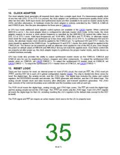
Figure 11-2. PRBS Output with Inverted RCLK Operation
RCINV = 1
RCLK
PRBS
PRBS DETECTOR
IS NOT IN SYNC
PRBS DETECTOR IS IN SYNC; THE
PRBS PIN PULSES HIGH FOR EACH BIT
ERROR DETECTED
11.2 Loopbacks
Each LIU has three internal loopbacks. See Figure 4-1 and Figure 4-2. The LLB and RLB pins (hardware mode) or
LLB and RLB control bits in the GCR register (CPU bus mode) enable these loopbacks. When LLB = RLB = 0,
loopbacks are disabled. Setting RLB = 1 with LLB = 0 enables remote loopback, which loops recovered clock and
data back through the LIU transmitter. During remote loopback, recovered clock and data are output on RCLK,
RPOS/RDAT, and RNEG/RLCV, but the TPOS/TDAT and TNEG pins are ignored. Setting LLB = 1 with RLB = 0
enables analog local loopback, which loops the outgoing transmit signal back to the receiver’s analog front end.
Setting LLB = RLB = 1 enables digital local loopback, which loops digital transmit clock and data back to the
receiver’s digital circuitry, including the LOS detector, the B3ZS/HDB3 decoder, and the PRBS detector. When
either of the local loopbacks is enabled, the transmit signal is output normally on TXP/TXN, but the received signal
on RXP/RXN is ignored.
34 of 71

 DALLAS [ DALLAS SEMICONDUCTOR ]