W134M/W134S
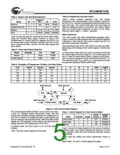
Table of Frequencies and Gear Ratios
Table 4. Bypass and Test Mode Selection
Bypclk
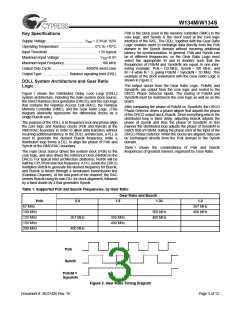
Table 6 shows several supported Pclk and Busclk
frequencies, the corresponding A and B dividers required in
the DRCG PLL, and the corresponding M and N dividers in the
gear ratio logic. The column Ratio gives the Gear Ratio as
defined Pclk/Synclk (same as M and N). The column F@PD
gives the divided down frequency (in MHz) at the Phase
Detector, where F@PD = Pclk/M = Synclk/N.
Mode
Normal
S0
0
S1
0
(int.)
Gnd
–
Clk
PAclk
Hi-Z
ClkB
PAclkB
Hi-Z
Output Test (OE)
Bypass
Test
0
1
1
1
0
1
PLLclk PLLclk PLLclkB
Refclk Refclk RefclkB
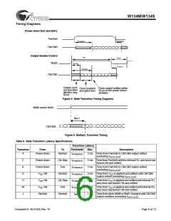
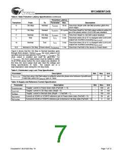
State Transitions
Table 5 shows the logic for selecting the Power-down mode,
using the PwrDnB input signal. PwrDnB is active LOW
(enabled when 0). When PwrDnB is disabled, the DRCG is in
its normal mode. When PwrDnB is enabled, the DRCG is put
into a powered-off state, and the Clk and ClkB outputs are
three-stated.
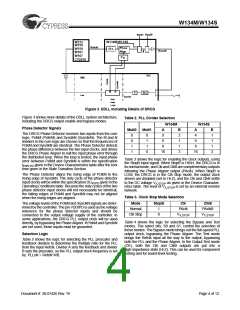
The clock source has three fundamental operating states.
Figure 4 shows the state diagram with each transition labelled
A through H. Note that the clock source output may NOT be
glitch-free during state transitions.
Upon powering up the device, the device can enter any state,
depending on the settings of the control signals, PwrDnB and
StopB.
Table 5. Power-down Mode Selection
In Power-down mode, the clock source is powered down with
the control signal, PwrDnB, equal to 0. The control signals S0
and S1 must be stable before power is applied to the device,
and can only be changed in Power-down mode (PwrDnB = 0).
The reference inputs, VDDR and VDDPD, may remain on or may
be grounded during the Power-down mode.
Mode
Normal
Power-down
PwrDnB
Clk
PAclk
GND
ClkB
PAclkB
GND
1
0
Table 6. Examples of Frequencies, Dividers, and Gear Ratios
Pclk
67
100
100
133
133
Refclk
33
50
50
67
Busclk
267
300
400
267
Synclk
67
75
100
67
100
A
8
6
8
4
6
B
1
1
1
1
1
M
2
8
4
4
8
N
2
6
4
2
6
Ratio
1.0
1.33
1.0
2.0
1.33
F@PD
33
12.5
25
33
16.7
67
400
VDD Turn-On
VDD Turn-On
G
J
M
L
Test
Normal
N
B
F
K
A
E
VDD Turn-On
H
VDD Turn-On
D
C
Power-Down
Clk Stop
Figure 4. Clock Source State Diagram
The control signals Mult0 and Mult1 can be used in two ways.
If they are changed during Power-down mode, then the
Power-down transition timings determine the settling time of
the DRCG. However, the Mult0 and Mult1 control signals can
also be changed during Normal mode. When the Mult control
signals are “hot-swapped” in this manner, the Mult transition
timings determine the settling time of the DRCG.
Table 7. Control Signals for Clock Source States
Clock
Output
State
Power-down
Clock Stop
Normal
PwrDnB
StopB
Source
Buffer
0
1
1
X
0
1
OFF
ON
ON
Ground
Disabled
Enabled
In Normal mode, the clock source is on, and the output is
enabled.
Figure 5 shows the timing diagrams for the various transitions
between states, and Table 8 specifies the latencies of each
state transition. Note that these transition latencies assume
the following.
Table 7 lists the control signals for each state.
Refclk input has settled and meets specification shown in
Table .
Mult0, Mult1, S0 and S1 control signals are stable.
Document #: 38-07426 Rev. *B
Page 5 of 12

 CYPRESS [ CYPRESS ]