W134M/W134S
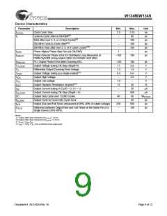
Device Characteristics
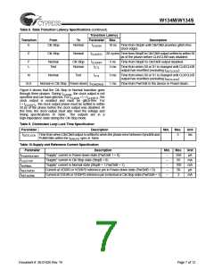
Parameter
tCYCLE
Description
Min.
2.5
–
–
–
Max.
3.75
60
100
100
160
–
Unit
ns
ps
ps
ps
Clock Cycle Time
tJ
Cycle-to-Cycle Jitter at Clk/ClkB[9]
Total Jitter over 2, 3, or 4 Clock Cycles[9]
266-MHz Cycle-to-Cycle Jitter[10]
266-MHz Total Jitter over 2, 3, or 4 Clock Cycles[10]
Phase Aligner Phase Step Size (at Clk/ClkB)
–
1
ps
ps
tSTEP
tERR,PD
Phase Detector Phase Error for Distributed Loop Measured at
–100
100
ps
PclkM-SynclkN (rising edges) (does not include clock jitter)
tERR,SSC
VX,STOP
VX
VCOS
VOH
VOL
rOUT
IOZ
IOZ,STOP
DC
PLL Output Phase Error when Tracking SSC
Output Voltage during Clk Stop (StopB=0)
Differential Output Crossing-Point Voltage
Output Voltage Swing (p-p single-ended)[11]
Output High Voltage
–100
1.1
1.3
0.4
–
1.0
12
–
–
40
–
250
–
100
2.0
1.8
0.6
2.0
–
50
50
500
60
50
ps
V
V
V
V
V
Output Low voltage
Output Dynamic Resistance (at pins)[12]
Output Current during Hi-Z (S0 = 0, S1 = 1)
Output Current during Clk Stop (StopB = 0)
Output Duty Cycle over 10,000 Cycles
Output Cycle-to-Cycle Duty Cycle Error
Output Rise and Fall Times (measured at 20%–80% of output voltage)
Ω
µA
µA
%tCYCLE
ps
tDC,ERR
tR,tF
tCR,CF
500
100
ps
ps
Difference between Output Rise and Fall Times on the Same Pin of a
Single Device (20%–80%)
Notes:
9. Output Jitter spec measured at t
10. Output Jitter Spec measured at t
= 2.5 ns.
CYCLE
CYCLE
= 3.75 ns.
11. V
= V –V
OH OL.
COS
12. r
= DV / D I . This is defined at the output pins.
O O
OUT
Document #: 38-07426 Rev. *B
Page 9 of 12

 CYPRESS [ CYPRESS ]