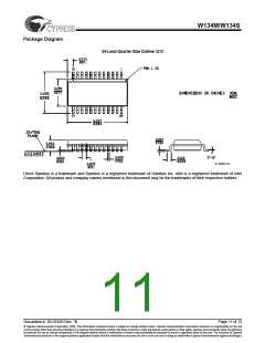
W134M/W134S
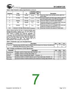
Table 8. State Transition Latency Specifications (continued)
Transition Latency
Transition
From
To
Parameter
Max.
Description
E
Clk Stop
Normal
tCLKON
10 ns Time from StopB until Clk/ClkB provides glitch-free
clock edges.
E
Clk Stop
Normal
tCLKSETL 20 cycles Time from StopB to Clk/ClkB output settled to within 50
ps of the phase before CLK/CLKB was disabled.
F
L
Normal
Test
Clk Stop
Normal
tCLKOFF
tCTL
5 ns
3 ms
Time from StopB to Clk/ClkB output disabled.
Time from when S0 or S1 is changed until CLK/CLKB
output has resettled (excluding tDISTLOCK).
N
Normal
Test
tCTL
3 ms
1 ms
Time from when S0 or S1 is changed until CLK/CLKB
output has resettled (excluding tDISTLOCK).
Time from PwrDnB to the device in Power-down.
B,D
Normal or Clk Stop Power-down tPOWERDN
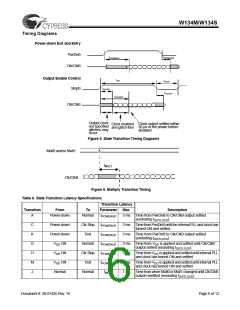
Figure 5 shows that the Clk Stop to Normal transition goes
through three phases. During tCLKON, the clock output is not
specified and can have glitches. For tCLKON < t < tCLKSETL, the
clock output is enabled and must be glitch-free. For
t > tCLKSETL, the clock output phase must be settled to within
50 ps of the phase before the clock output was disabled. At
this time, the clock output must also meet the voltage and
timing specifications of Table . The outputs are in a
high-impedance state during the Clk Stop mode.
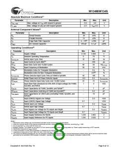
Table 9. Distributed Loop Lock Time Specification
Parameter
Description
Min.
Max.
Unit
tDISTLOCK Time from when Clk/ClkB output is settled to when the phase error between SynclkN and
5
ms
PclkM falls within the tERR,PD spec in Table .
Table 10.Supply and Reference Current Specification
Parameter
IPOWERDOWN
ICLKSTOP
INORMAL
IREF,PWDN
IREF,NORM
Description
Min.
Max.
250
65
100
50
Unit
µA
mA
mA
µA
“Supply” current in Power-down state (PwrDnB 1 = 0)
“Supply” current in Clk Stop state (StopB = 0)
“Supply” current in Normal state (StopB = 1,PwrDnB = 1)
Current at VDDIR or VDDIPD reference pin in Power-down state (PwrDnB = 0)
Current at VDDIR or VDDIPD reference pin in Normal or Clk Stop state (PwrDnB = 1)
–
–
–
–
–
2
mA
Document #: 38-07426 Rev. *B
Page 7 of 12

 CYPRESS [ CYPRESS ]