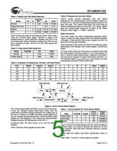
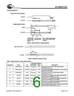
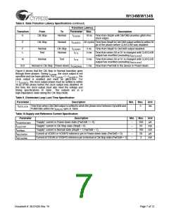
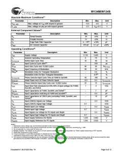
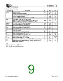
W134M/W134S
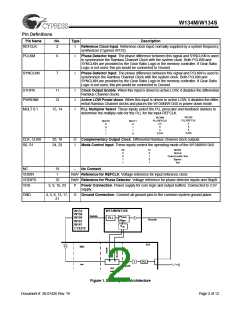
Pin Definitions
Pin Name
No.
Type
Description
REFCLK
2
I
Reference Clock Input. Reference clock input, normally supplied by a system frequency
synthesizer (Cypress W133).
PCLKM
6
7
I
I
Phase Detector Input. The phase difference between this signal and SYNCLKN is used
to synchronize the Rambus Channel Clock with the system clock. Both PCLKM and
SYNCLKN are provided by the Gear Ratio Logic in the memory controller. If Gear Ratio
Logic is not used, this pin would be connected to Ground.
Phase Detector Input. The phase difference between this signal and PCLKM is used to
synchronize the Rambus Channel Clock with the system clock. Both PCLKM and
SYNCLKN are provided by the Gear Ratio Logic in the memory controller. If Gear Ratio
Logic is not used, this pin would be connected to Ground.
SYNCLKN
STOPB
11
12
I
I
I
Clock Output Enable. When this input is driven to active LOW, it disables the differential
Rambus Channel clocks.
PWRDNB
MULT 0:1
Active LOW Power-down. When this input is driven to active LOW, it disables the differ-
ential Rambus Channel clocks and places the W134M/W134S in power-down mode.
15, 14
PLL Multiplier Select. These inputs select the PLL prescaler and feedback dividers to
determine the multiply ratio for the PLL for the input REFCLK.
W134S
W134M
PLL/REFCLK
PLL/REFCLK
MULT0
MULT1
4
6
8
4.5
6
8
0
0
1
1
0
1
1
0
5.333
5.333
CLK, CLKB
S0, S1
20, 18
24, 23
O
I
Complementary Output Clock. Differential Rambus Channel clock outputs.
Mode Control Input. These inputs control the operating mode of the W134M/W134S.
MODE
Normal
S0
0
S1
0
Output Enable Test
Bypass
0
1
1
1
0
1
Test
NC
VDDIR
VDDIPD
19
1
10
–
No Connect
RefV Reference for REFCLK. Voltage reference for input reference clock.
RefV Reference for Phase Detector. Voltage reference for phase detector inputs and StopB.
VDD
3, 9, 16, 22
P
Power Connection. Power supply for core logic and output buffers. Connected to 3.3V
supply.
GND
4, 5, 8, 13, 17,
21
G
Ground Connection. Connect all ground pins to the common system ground plane.
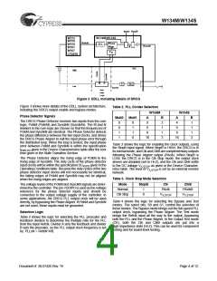
W134M/W134S
W133
W158
W159
W161
W167
Refclk
Phase
PLL
Busclk
Align
D
CY2210
RAC
RMC
Pclk
M
N
4
DLL
Synclk
Gear
Ratio
Logic
Figure 1. DDLL System Architecture
Document #: 38-07426 Rev. *B
Page 2 of 12

 CYPRESS [ CYPRESS ]