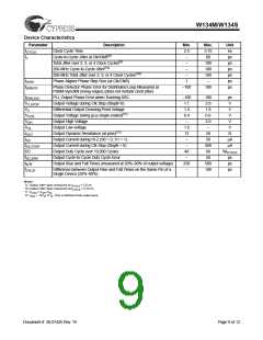
W134M/W134S
StopB
S0/S1
W134M/W134S
W133
W158
W159
W161
W167
Refclk
Phase
PLL
Busclk
Align
D
CY2210
RAC
RMC
Pclk
M
N
4
DLL
Synclk
Gear
Ratio
Logic
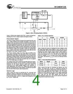
Figure 3. DDLL Including Details of DRCG
Figure 3 shows more details of the DDLL system architecture,
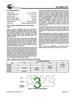
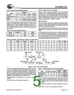
Table 2. PLL Divider Selection
W134M
including the DRCG output enable and bypass modes.
W134S
Phase Detector Signals
Mult0
Mult1
A
9
6
8
16
B
2
1
1
3
A
4
6
8
16
B
1
1
1
3
The DRCG Phase Detector receives two inputs from the core
logic, PclkM (Pclk/M) and SynclkN (Synclk/N). The M and N
dividers in the core logic are chosen so that the frequencies of
PclkM and SynclkN are identical. The Phase Detector detects
the phase difference between the two input clocks, and drives
the DRCG Phase Aligner to null the input phase error through
the distributed loop. When the loop is locked, the input phase
error between PclkM and SynclkN is within the specification
0
0
1
1
0
1
1
0
Table 3 shows the logic for enabling the clock outputs, using
the StopB input signal. When StopB is HIGH, the DRCG is in
its normal mode, and Clk and ClkB are complementary outputs
following the Phase Aligner output (PAclk). When StopB is
LOW, the DRCG is in the Clk Stop mode, the output clock
drivers are disabled (set to Hi-Z), and the Clk and ClkB settle
to the DC voltage VX,STOP as given in the Device Character-
istics table. The level of VX,STOP is set by an external resistor
network.
t
ERR,PD given in the Device Characteristics table after the lock
time given in the State Transition Section.
The Phase Detector aligns the rising edge of PclkM to the
rising edge of SynclkN. The duty cycle of the phase detector
input clocks will be within the specification DCIN,PD given in the
Operating Conditions table. Because the duty cycles of the two
phase detector input clocks will not necessarily be identical,
the falling edges of PclkM and SynclkN may not be aligned
when the rising edges are aligned.
Table 3. Clock Stop Mode Selection
The voltage levels of the PclkM and SynclkN signals are deter-
mined by the controller. The pin VDDIPD is used as the voltage
reference for the phase detector inputs and should be
connected to the output voltage supply of the controller. In
some applications, the DRCG PLL output clock will be used
directly, by bypassing the Phase Aligner. If PclkM and SynclkN
are not used, those inputs must be grounded.
Mode
Normal
Clk Stop
StopB
Clk
PAclk
VX,STOP
ClkB
PAclkB
VX,STOP
1
0
Table 4 shows the logic for selecting the Bypass and Test
modes. The select bits, S0 and S1, control the selection of
these modes. The Bypass mode brings out the full-speed PLL
output clock, bypassing the Phase Aligner. The Test mode
brings the Refclk input all the way to the output, bypassing
both the PLL and the Phase Aligner. In the Output Test mode
(OE), both the Clk and ClkB outputs are put into a
high-impedance state (Hi-Z). This can be used for component
testing and for board-level testing.
Selection Logic
Table 2 shows the logic for selecting the PLL prescaler and
feedback dividers to determine the multiply ratio for the PLL
from the input Refclk. Divider A sets the feedback and divider
B sets the prescaler, so the PLL output clock frequency is set
by: PLLclk = Refclk*A/B.
Document #: 38-07426 Rev. *B
Page 4 of 12

 CYPRESS [ CYPRESS ]