W134M/W134S
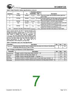
Absolute Maximum Conditions[1]
Parameter
VDD, ABS
VI, ABS
Description
Max. voltage on VDD with respect to ground
Max. voltage on any pin with respect ground
Min.
–0.5
–0.5
Max.
4.0
VDD+0.5
Unit
V
V
External Component Values[2]
Parameter
Description
Min.
39
Max.
±5%
Unit
Ω
RS
Serial Resistor
RP
CF
CMID
Parallel Resistor
Edge Rate Filter Capacitor
AC Ground Capacitor
51
±5%
±10%
0.1 µF
Ω
4 – 15[3]
470 pF
pF
±20%
Operating Conditions[4]
Parameter
VDD
TA
Description
Min.
3.135
0
Max.
3.465
70
Unit
V
°C
Supply Voltage
Ambient Operating Temperature
tCYCLE,IN
tJ,IN
Refclk Input Cycle Time
10
–
40
30
–
40
250
60
ns
ps
%tCYCLE
kHz
Input Cycle-to-Cycle Jitter[5]
DCIN
FMIN
PMIN
Input Duty Cycle over 10,000 Cycles
Input Frequency of Modulation
33
[6]
Modulation Index for Triangular Modulation
Modulation Index for Non-Triangular Modulation
Phase Detector Input Cycle Time at PclkM & SynclkN
Initial Phase error at Phase Detector Inputs
Phase Detector Input Duty Cycle over 10,000 Cycles
0.6
0.5[8]
100
0.5
75
%
%
ns
–
tCYCLE,PD
tERR,INIT
DCIN,PD
tI,SR
30
–0.5
25
1
tCYCLE,PD
tCYCLE,PD
V/ns
Input Slew Rate (measured at 20%-80% of input voltage) for PclkM,
4
SynclkN, and Refclk
CIN,PD
DCIN,PD
CIN,CMOS
Input Capacitance at PclkM, SynclkN, and Refclk[7]
Input Capacitance matching at PclkM and SynclkN[7]
–
–
–
7
0.5
10
pF
pF
pF
Input Capacitance at CMOS pins (excluding PclkM, SynclkN, and
Refclk)[7]
VIL
VIH
Input (CMOS) Signal Low Voltage
Input (CMOS) Signal High Voltage
Refclk input Low Voltage
–
0.7
–
0.7
–
0.7
1.235
1.235
0.3
–
0.3
–
0.3
–
3.465
2.625
VDD
VDD
VDDIR
VDDIR
VDDIPD
VDDIPD
V
VIL,R
VIH,R
VIL,PD
VIH,PD
VDDIR
VDDIPD
Refclk input High Voltage
Input Signal Low Voltage for PD Inputs and StopB
Input Signal High Voltage for PD Inputs and StopB
Input Supply Reference for Refclk
Input Supply Reference for PD Inputs
V
Notes:
1. Represents stress ratings only, and functional operation at the maximums is not guaranteed.
2. Gives the nominal values of the external components and their maximum acceptable tolerance, assuming Z = 28Ω.
CH
3. Do not populate C . Leave pads for future use.
F
4. Multiple Supplies: The voltage on any input or I/O pin cannot exceed the power pin during power-up. Power supply sequencing is NOT required.
5. Refclk jitter measured at V (nom)/2.
DDIR
6. If input modulation is used: input modulation is allowed but not required.
7. Capacitance measured at Freq=1 MHz, DC bias = 0.9V and V < 100 mV.
AC
8. The amount of allowed spreading for any non-triangular modulation is determined by the induced downstream tracking skew, which cannot exceed the skew
generated by the specified 0.6% triangular modulation. Typically, the amount of allowed non-triangular modulation is about 0.5%.
Document #: 38-07426 Rev. *B
Page 8 of 12

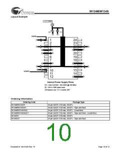
 CYPRESS [ CYPRESS ]