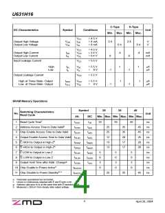
U631H16
Device Operation
parallel programming of all nonvolatile elements. Once
a STORE cycle is initiated, further inputs and outputs
are disabled until the cycle is completed.
The U631H16 has two separate modes of operation:
SRAM mode and nonvolatile mode. In SRAM mode,
the memory operates as a standard fast static RAM. In
nonvolatile mode, data is transferred from SRAM to
EEPROM (the STORE operation) or from EEPROM to
SRAM (the RECALL operation). In this mode SRAM
functions are disabled.
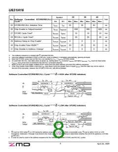
Because a sequence of addresses is used for STORE
initiation, it is important that no other READ or WRITE
accesses intervene in the sequence or the sequence
will be aborted and no STORE or RECALL will take
place.
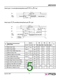
To initiate the STORE cycle the following READ
sequence must be performed:
SRAM READ
1.
2.
3.
4.
5.
6.
Read address
Read address
Read address
Read address
Read address
Read address
000
555
(hex) Valid READ
(hex) Valid READ
The U631H16 performs a READ cycle whenever E and
G are LOW while W is HIGH. The address specified on
pins A0 - A10 determines which of the 2048 data bytes
will be accessed. When the READ is initiated by an
address transition, the outputs will be valid after a delay
of tcR. If the READ is initiated by E or G, the outputs will
be valid at ta(E) or at ta(G), whichever is later. The data
outputs will repeatedly respond to address changes
within the tcR access time without the need for transition
on any control input pins, and will remain valid until
another address change or until E or G is brought
HIGH or W is brought LOW.
2AA (hex) Valid READ
7FF
0F0
70F
(hex) Valid READ
(hex) Valid READ
(hex) Initiate STORE
Once the sixth address in the sequence has been
entered, the STORE cycle will commence and the chip
will be disabled. It is important that READ cycles and
not WRITE cycles are used in the sequence. It is not
necessary that G is LOW for the sequence to be valid.
After the tSTORE cycle time has been fulfilled, the SRAM
will again be activated for READ and WRITE operation.
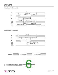
SRAM WRITE
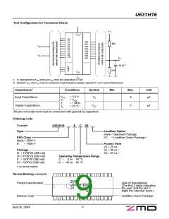
Software Nonvolatile RECALL
A WRITE cycle is performed whenever E and W are
LOW. The address inputs must be stable prior to
entering the WRITE cycle and must remain stable until
ei-ther E or W goes HIGH at the end of the cycle. The
data on pins DQ0 - 7 will be written into the memory if it
is valid tsu(D) before the end of a W controlled WRITE or
A RECALL cycle of the EEPROM data into the SRAM
is initiated with a sequence of READ operations in a
manner similar to the STORE initiation. To initiate the
RECALL cycle the following sequence of READ opera-
tions must be performed:
t
su(D) before the end of an E controlled WRITE.
It is recommended that G is kept HIGH during the
entire WRITE cycle to avoid data bus contention on the
common I/O lines. If G is left LOW, internal circuitry will
turn off the output buffers tdis(W) after W goes LOW.
1.
2.
3.
4.
5.
6.
Read address
Read address
Read address
Read address
Read address
Read address
000
555
(hex) Valid READ
(hex) Valid READ
2AA (hex) Valid READ
7FF
0F0
70E
(hex) Valid READ
(hex) Valid READ
(hex) Initiate RECALL
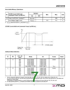
Noise Consideration
The U631H16 is a high speed memory and therefore it
must have a high frequency bypass capacitor of appro-
ximately 0.1 µF connected between VCC and VSS using
leads and traces that are as short as possible. As with
all high speed CMOS ICs, normal carefull routing of
power, ground and signals will help prevent noise pro-
blems.
Internally, RECALL is a two step procedure. First, the
SRAM data is cleared and second, the nonvolatile
information is transferred into the SRAM cells. The
RECALL operation in no way alters the data in the
EEPROM cells. The nonvolatile data can be recalled an
unlimited number of times.
Automatic Power Up RECALL
Software Nonvolatile STORE
On power up, once VCC exceeds the sense voltage of
The U631H16 software controlled STORE cycle is
initiated by executing sequential READ cycles from six
specific address locations. By relying on READ cycles
only, the U631H16 implements nonvolatile operation
while remaining compatible with standard 2K x 8
SRAMs. During the STORE cycle, an erase of the pre-
vious nonvolatile data is first performed, followed by
VSWITCH, a RECALL cycle is automatically initiated. The
voltage on the VCC pin must not frop belwo VSWITCH
once it has risen above it in order for the RECALL to
operate properly. Due to this automatic RECALL,
SRAM operation cannot commence until tRESTORE after
V
CC exceeds VSWITCH.
10
April 20, 2004

 CYPRESS [ CYPRESS ]