SL811HS
5.3.2
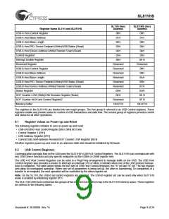
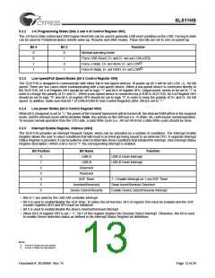
J-K Programming States [bits 3 and 4 of Control Register 05H]
The J-K force state control and USB Engine Reset bits can be used to generate USB reset condition on the USB. Forcing K-state
can be used for Peripheral device remote wake-up, Resume and other modes. These two bits are set to zero on power-up.
Bit 4
Bit 3
Function
0
0
1
1
0
1
0
1
Normal operating mode
Force USB Reset, D+ and D– are set LOW (SE0)
Force J-State, D+ set HIGH, D– set LOW[2]
Force K-State, D– set HIGH, D+ set LOW[3]
5.3.3
Low-speed/Full Speed Modes [bit 5 Control Register 05H]
The SL811HS is designed to communicate with either full or low-speed devices. At power-up bit 5 will be set LOW, i.e., for full
speed. There are two cases when communicating with a low-speed device. When a low-speed device is connected directly to
the SL811HS, bit 5 of Register 05H should be set to logic “1” and bit 6 of register 0FH, Output-Invert, needs to be set to “1” in
order to change the polarity of D+ and D–. When a low-speed device is connected via a HUB to SL811HS, bit 5 of Register 05H
should be set to logic “0” and bit 6 of register 0FH should be set to logic “0” in order to keep the polarity of D+ and D– for full
speed. In addition, make sure that bit 7 of USB-A/USB-B Host Control Registers [00H, 08H] is set to “1.”
5.3.4
Low-power Modes [bit 6 Control Register 05H]
When bit-6 (Suspend) is set to “1,” the power of the transmit transceiver will be turned off, the internal RAM will be in the suspend
mode, and the internal clocks will be disabled. Note. Any activity on the USB bus (i.e., K-State, etc.) will resume normal operation.
To resume normal operation from the CPU side, a data Write cycle (i.e., A0 set HIGH for a data Write cycle) should be done.
5.3.5
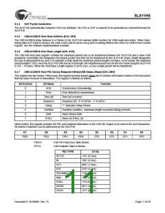
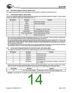
Interrupt Enable Register, Address [06H]
The SL811HS provides an Interrupt Request Output, which can be activated on a number of conditions. The Interrupt Enable
Register allows the user to select conditions that will result in an Interrupt being issued to an external CPU. A separate Interrupt
Status Register is provided. It can be polled in order to determine those conditions that initiated the interrupt. (See Interrupt Status
Register description.) When a bit is set to “1” the corresponding interrupt is enabled.
Bit Position
Bit Name
USB-A
Function
0
1
2
3
4
5
6
USB-A Done Interrupt
USB-B Done Interrupt
USB-B
Reserved
Reserved
SOF Timer
1 = Enable Interrupt on 1-ms SOF Timer
Slave Insert/Remove Detection
Inserted/Removed
Device Detect/Resume
Enable Device Detect/Resume Interrupt
• Bits 0–1 are used for the USB A/B controller interrupt.
• Bit 4 is used to enable/disable the SOF timer. To utilize this bit function, bit 0 of register 05H must be enabled and the SOF
counter registers 0EH and 0FH must be initialized.
• Bit 5 is used to enable/disable the device inserted/removed interrupt.
• When bit-6 of register 05H is set = “1,” bit 6 of this register enables the Resume Detect Interrupt. Otherwise, this bit is used
to enable Device detection status as defined in the Interrupt Status Register bit definitions.
Note:
2. Force K-State for low speed.
3. Force J-State for low speed.
Document #: 38-08008 Rev. *A
Page 13 of 29

 CYPRESS [ CYPRESS ]