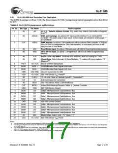
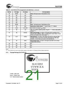
SL811HS
6.1.3
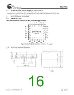
SL811HS USB Host Controller Pins Description
The SL811HS package is a 28-pin PLCC. The device requires 3.3 VDC. Average typical current consumption is less then 20 mA
for 3.3V.
Table 6-1. SL811HS Pin Assignments and Definitions
Pin No. Pin Type
Pin Name
Pin Description
1
IN
A0
A0 = “0.” Selects Address Pointer. Reg. Write Only. Selects Data Buffer or Register.
R/W.[4]
2
IN
nDACK
nDRQ
DMA Acknowledge. An active LOW input used to interface to an external DMA
controller. This works only in slave mode. In host mode, pin should be tied to Logic “1”
in Host Mode.
3
OUT
DMA Request. An active LOW output used with an external DMA controller. nDRQ and
nDACK form the handshake for DMA data transfers. In host mode, pin must be left
unconnected in Host Mode.
4
5
IN
IN
nRD
Read Strobe Input. An active LOW input used with nCS to Read registers/data memory.
nWR
Write Strobe Input. An active LOW input used with nCS to Write to registers/data
memory.
6
7
IN
IN
nCS
CM
Active LOW Chip Select. Used with nRD and nWD when accessing SL811HS.
Clock Mode. Select Internal 4 X Clock Multiplier. “1” enables 4X clock multiplier. “0”
Disables.[5]
8
VDD1
BIDIR
BIDIR
GND
VDD
IN
+3.3 VDC
DATA +
DATA -
Power for USB Transceivers
9
USB Differential Data Signal HIGH Side
USB Differential Data Signal LOW Side
10
11
12
13
14
15
16
17
18
19
20
21
22
23
24
25
26
27
28
USB GND Ground Connection for USB
+3.3 VDC SL811HS Device VDD Power[6]
CLK/X1
X2
12-/48-MHz Clock or External Crystal X1 Connection[7]
OUT
IN
External Crystal X2 Connection
nRST
INTRQ
GND
D0
SL811HS Device Active LOW Reset Input
Active HIGH Interrupt Request Output to External Controller
SL811HS Device Ground
OUT
GND
BIDIR
BIDIR
BIDIR
BIDIR
GND
BIDIR
BIDIR
BIDIR
BIDIR
IN
Data 0. Microprocessor Data/(Address) Bus
Data 1. Microprocessor Data/(Address) Bus
Data 2. Microprocessor Data/(Address) Bus
Data 3. Microprocessor Data/(Address) Bus
SL811HS Device Ground
D1
D2
D3
GND
D4
Data 4. Microprocessor Data/(Address) Bus
Data 5. Microprocessor Data/(Address) Bus
Data 6. Microprocessor Data/(Address) Bus
Data 7. Microprocessor Data/(Address) Bus
Master/Slave Select. Host = “0,” Slave = “1”
D5
D6
D7
M/S
VDD
+3.3 VDC SL811HS Device VDD Power
Notes:
4. The A0 Address bit is used to access address or data registers in I/O-mapped or memory-mapped applications.
5. The CM Clock Multiplier pin should be tied HIGH for a 12-MHz clock source and tied to ground for a 48-MHz clock source. In SL11H, this pin was designated
as an ALE input pin.
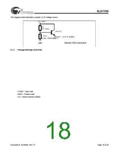
6. VDD can be derived from the USB supply. The diagram below shows a simple method to provide 3.3V/30 mA. Another option is to use a Torex Semiconductor,
Ltd. 3.3V SMD regulator (part number XC62HR3302MR).
7. The X1/X2 clock requires external 12- or 48-MHz matching crystal or clock source.
Document #: 38-08008 Rev. *A
Page 17 of 29

 CYPRESS [ CYPRESS ]