PSoC® 3: CY8C32 Family
Data Sheet
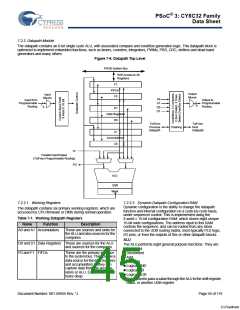
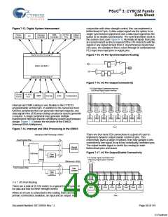
Figure 7-13. Digital System Interconnect
conjunction with drive strength control, this can implement a
bidirectional I/O pin. A data output signal has the option to be
single synchronized (pipelined) and a data input signal has the
option to be double synchronized. The synchronization clock is
the system clock (see Figure 6-1). Normally all inputs from pins
are synchronized as this is required if the CPU interacts with the
signal or any signal derived from it. Asynchronous inputs have
rare uses. An example of this is a feed through of combinational
PLD logic from input pins to output pins.
Timers
Interrupt
DMA
IO Port
Pins
Global
Clocks
I2C
Counters
Controller
Controller
Digital System Routing I/F
UDB ARRAY
Figure 7-15. I/O Pin Synchronization Routing
DO
DI
Digital System Routing I/F
Figure 7-16. I/O Pin Output Connectivity
8 IO Data Output Connections from the
UDB Array Digital System Interface
Global
Clocks
I/O Port
Pins
EMIF
Del-Sig
DAC
Comparators
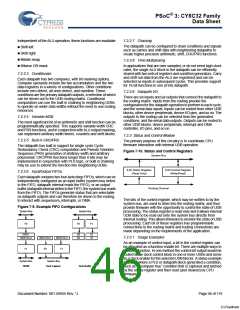
Interrupt and DMA routing is very flexible in the CY8C32
programmable architecture. In addition to the numerous fixed
function peripherals that can generate interrupt requests, any
data signal in the UDB array routing can also be used to generate
a request. A single peripheral may generate multiple
independent interrupt requests simplifying system and firmware
design. Figure 7-14 shows the structure of the IDMUX
(Interrupt/DMA Multiplexer).
DO
PIN 0
DO
PIN1
DO
PIN2
DO
PIN3
DO
DO
PIN5
DO
PIN6
DO
PIN7
PIN4
Port i
Figure 7-14. Interrupt and DMA Processing in the IDMUX
Interrupt and DMA Processing in IDMUX
There are four more DSI connections to a given I/O port to
implement dynamic output enable control of pins. This
connectivity gives a range of options, from fully ganged 8-bits
controlled by one signal, to up to four individually controlled pins.
The output enable signal is useful for creating tri-state
bidirectional pins and buses.
Fixed Function IRQs
0
1
Interrupt
Controller
IRQs
2
3
Figure 7-17. I/O Pin Output Enable Connectivity
UDB Array
Edge
Detect
4 IO Control Signal Connections from
UDB Array Digital System Interface
DRQs
DMA termout (IRQs)
0
Fixed Function DRQs
DMA
Controller
1
2
Edge
Detect
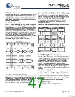
7.4.1 I/O Port Routing
OE
PIN 0
OE
PIN1
OE
PIN2
OE
PIN3
OE
PIN4
OE
PIN5
OE
PIN6
OE
PIN7
There are a total of 20 DSI routes to a typical 8-bit I/O port, 16
for data and four for drive strength control.
When an I/O pin is connected to the routing, there are two
primary connections available, an input and an output. In
Port i
Document Number: 001-56955 Rev. *J
Page 48 of 119
[+] Feedback

 CYPRESS [ CYPRESS ]