PSoC® 3: CY8C32 Family
Data Sheet
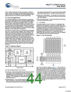
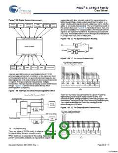
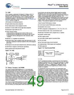
7.2.2 Datapath Module
The datapath contains an 8-bit single cycle ALU, with associated compare and condition generation logic. This datapath block is
optimized to implement embedded functions, such as timers, counters, integrators, PWMs, PRS, CRC, shifters and dead band
generators and many others.
Figure 7-8. Datapath Top Level
PHUB System Bus
R/W Access to All
Registers
F1
FIFOs
Output
Muxes
Input
Muxes
F0
A0
A1
D0
D1
Input from
Programmable
Routing
Output to
Programmable
Routing
6
6
D1
Data Registers
D0
To/From
Previous
Datapath
To/From
Next
Datapath
Chaining
A1
Accumulators
A0
PI
Parallel Input/Output
(To/From Programmable Routing)
PO
ALU
Shift
Mask
7.2.2.1 Working Registers
7.2.2.2 Dynamic Datapath Configuration RAM
Dynamic configuration is the ability to change the datapath
function and internal configuration on a cycle-by-cycle basis,
under sequencer control. This is implemented using the
8-word × 16-bit configuration RAM, which stores eight unique
16-bit wide configurations. The address input to this RAM
controls the sequence, and can be routed from any block
connected to the UDB routing matrix, most typically PLD logic,
I/O pins, or from the outputs of this or other datapath blocks.
The datapath contains six primary working registers, which are
accessed by CPU firmware or DMA during normal operation.
Table 7-1. Working Datapath Registers
Name
Function
Description
A0 and A1 Accumulators
These are sources and sinks for
the ALU and also sources for the
compares.
ALU
D0 and D1 Data Registers These are sources for the ALU
and sources for the compares.
The ALU performs eight general purpose functions. They are:
Increment
F0 and F1 FIFOs
These are the primary interface
to the system bus. They can be a
data source for the data registers
and accumulators or they can
capture data from the accumu-
lators or ALU. Each FIFO is four
bytes deep.
Decrement
Add
Subtract
Logical AND
Logical OR
Logical XOR
Pass, used to pass a value through the ALU to the shift register,
mask, or another UDB register
Document Number: 001-56955 Rev. *J
Page 45 of 119
[+] Feedback

 CYPRESS [ CYPRESS ]