PSoC® 3: CY8C32 Family
Data Sheet
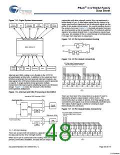
PSoC Creator contains all the tools necessary to complete a
design, and then to maintain and extend that design for years to
come. All steps of the design flow are carefully integrated and
optimized for ease-of-use and to maximize productivity.
alsocontainsinput/outputFIFOs,whicharetheprimaryparallel
data interface between the CPU/DMA system and the UDB.
Status and Control Module – The primary role of this block is
to provide a way for CPU firmware to interact and synchronize
with UDB operation.
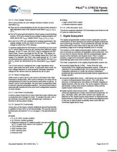
7.2 Universal Digital Block
Clock and Reset Module – This block provides the UDB clocks
and reset selection and control.
The Universal Digital Block (UDB) represents an evolutionary
step to the next generation of PSoC embedded digital peripheral
functionality. The architecture in first generation PSoC digital
blocks provides coarse programmability in which a few fixed
functions with a small number of options are available. The new
UDB architecture is the optimal balance between configuration
granularity and efficient implementation. A cornerstone of this
approach is to provide the ability to customize the devices digital
operation to match application requirements.
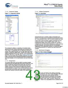
7.2.1 PLD Module
The primary purpose of the PLD blocks is to implement logic
expressions, state machines, sequencers, lookup tables, and
decoders. In the simplest use model, consider the PLD blocks as
a standalone resource onto which general purpose RTL is
synthesized and mapped. The more common and efficient use
model is to create digital functions from a combination of PLD
and datapath blocks, where the PLD implements only the
random logic and state portion of the function while the datapath
(ALU) implements the more structured elements.
To achieve this, UDBs consist of a combination of uncommitted
logic (PLD), structured logic (Datapath), and a flexible routing
scheme to provide interconnect between these elements, I/O
connections, and other peripherals. UDB functionality ranges
from simple self contained functions that are implemented in one
UDB, or even a portion of a UDB (unused resources are
available for other functions), to more complex functions that
require multiple UDBs. Examples of basic functions are timers,
counters, CRC generators, PWMs, dead band generators, and
communications functions, such as UARTs, SPI, and I2C. Also,
the PLD blocks and connectivity provide full featured general
purpose programmable logic within the limits of the available
resources.
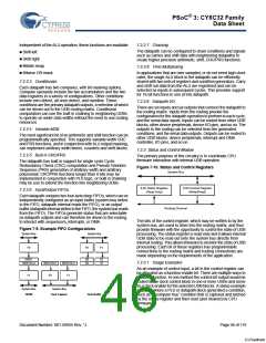
Figure 7-7. PLD 12C4 Structure
IN0
IN1
IN2
IN3
IN4
IN5
IN6
IN7
IN8
IN9
IN10
IN11
T C T C T C T C T C T C T C T C
T C T C T C T C T C T C T C T C
T C T C T C T C T C T C T C T C
T C T C T C T C T C T C T C T C
T C T C T C T C T C T C T C T C
T C T C T C T C T C T C T C T C
T C T C T C T C T C T C T C T C
T C T C T C T C T C T C T C T C
T C T C T C T C T C T C T C T C
T C T C T C T C T C T C T C T C
T C T C T C T C T C T C T C T C
T C T C T C T C T C T C T C T C
AND
Array
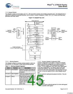
Figure 7-6. UDB Block Diagram
PLD
Chaining
PLD
12C4
(8 PTs)
PLD
12C4
(8 PTs)
Clock
and Reset
Control
SELIN
(carry in)
OUT0
OUT1
OUT2
OUT3
MC0
MC1
MC2
MC3
T
T
T
T
T
T
T
T
T
T
T
T
T
T
T
T
T
T
T
T
T
T
T
T
T
T
T
T
T
T
T
T
Status and
Control
Datapath
Datapath
Chaining
SELOUT
(carry out)
OR
Array
One 12C4 PLD block is shown in Figure 7-7. This PLD has 12
inputs, which feed across eight product terms. Each product term
(AND function) can be from 1 to 12 inputs wide, and in a given
product term, the true (T) or complement (C) of each input can
be selected. The product terms are summed (OR function) to
create the PLD outputs. A sum can be from 1 to 8 product terms
wide. The 'C' in 12C4 indicates that the width of the OR gate (in
this case 8) is constant across all outputs (rather than variable
as in a 22V10 device). This PLA like structure gives maximum
flexibility and insures that all inputs and outputs are permutable
for ease of allocation by the software tools. There are two 12C4
PLDs in each UDB.
Routing Channel
The main component blocks of the UDB are:
PLD blocks – There are two small PLDs per UDB. Theseblocks
take inputs from the routing array and form registered or
combinational sum-of-products logic. PLDs are used to
implement state machines, state bits, and combinational logic
equations. PLD configuration is automatically generated from
graphical primitives.
DatapathModule–This8-bitwidedatapathcontainsstructured
logic to implement a dynamically configurable ALU, a variety
ofcompare configurations andconditiongeneration. Thisblock
Document Number: 001-56955 Rev. *J
Page 44 of 119
[+] Feedback

 CYPRESS [ CYPRESS ]