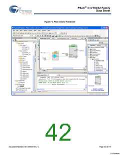
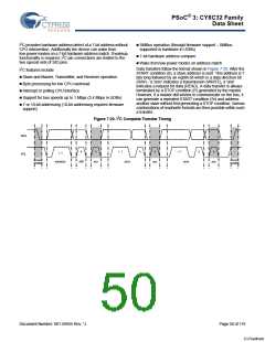
PSoC® 3: CY8C32 Family
Data Sheet
Independent of the ALU operation, these functions are available:
7.2.2.7 Chaining
The datapath can be configured to chain conditions and signals
such as carries and shift data with neighboring datapaths to
create higher precision arithmetic, shift, CRC/PRS functions.
Shift left
Shift right
Nibble swap
Bitwise OR mask
7.2.2.8 Time Multiplexing
In applications that are over sampled, or do not need high clock
rates, the single ALU block in the datapath can be efficiently
shared with two sets of registers and condition generators. Carry
and shift out data from the ALU are registered and can be
selected as inputs in subsequent cycles. This provides support
for 16-bit functions in one (8-bit) datapath.
7.2.2.3 Conditionals
Each datapath has two compares, with bit masking options.
Compare operands include the two accumulators and the two
data registers in a variety of configurations. Other conditions
include zero detect, all ones detect, and overflow. These
conditions are the primary datapath outputs, a selection of which
can be driven out to the UDB routing matrix. Conditional
computation can use the built in chaining to neighboring UDBs
to operate on wider data widths without the need to use routing
resources.
7.2.2.9 Datapath I/O
There are six inputs and six outputs that connect the datapath to
the routing matrix. Inputs from the routing provide the
configuration for the datapath operation to perform in each cycle,
and the serial data inputs. Inputs can be routed from other UDB
blocks, other device peripherals, device I/O pins, and so on. The
outputs to the routing can be selected from the generated
conditions, and the serial data outputs. Outputs can be routed to
other UDB blocks, device peripherals, interrupt and DMA
controller, I/O pins, and so on.
7.2.2.4 Variable MSB
The most significant bit of an arithmetic and shift function can be
programmatically specified. This supports variable width CRC
and PRS functions, and in conjunction with ALU output masking,
can implement arbitrary width timers, counters and shift blocks.
7.2.3 Status and Control Module
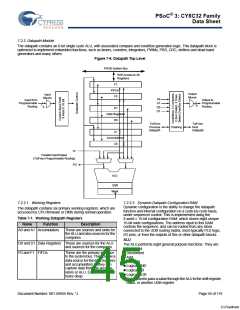
7.2.2.5 Built in CRC/PRS
The primary purpose of this circuitry is to coordinate CPU
firmware interaction with internal UDB operation.
The datapath has built in support for single cycle Cyclic
Redundancy Check (CRC) computation and Pseudo Random
Sequence (PRS) generation of arbitrary width and arbitrary
polynomial. CRC/PRS functions longer than 8 bits may be
implemented in conjunction with PLD logic, or built in chaining
may be use to extend the function into neighboring UDBs.
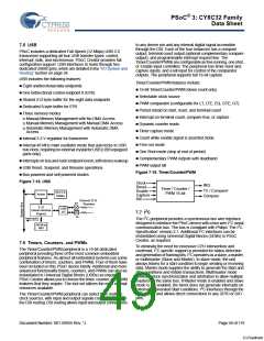
Figure 7-10. Status and Control Registers
System Bus
8-bit Status Register
(Read Only)
8-bit Control Register
(Write/Read)
7.2.2.6 Input/Output FIFOs
Each datapath contains two four-byte deep FIFOs, which can be
independently configured as an input buffer (system bus writes
to the FIFO, datapath internal reads the FIFO), or an output
buffer (datapath internal writes to the FIFO, the system bus reads
from the FIFO). The FIFOs generate status that are selectable
as datapath outputs and can therefore be driven to the routing,
to interact with sequencers, interrupts, or DMA.
Routing Channel
The bits of the control register, which may be written to by the
system bus, are used to drive into the routing matrix, and thus
provide firmware with the opportunity to control the state of UDB
processing. The status register is read-only and it allows internal
UDB state to be read out onto the system bus directly from
internal routing. This allows firmware to monitor the state of UDB
processing. Each bit of these registers has programmable
connections to the routing matrix and routing connections are
made depending on the requirements of the application.
Figure 7-9. Example FIFO Configurations
System Bus
System Bus
F0
F0
F1
D0/D1
D0
A0
D1
A1
7.2.3.1 Usage Examples
A0/A1/ALU
A0/A1/ALU
F0
A0/A1/ALU
F1
As an example of control input, a bit in the control register can
be allocated as a function enable bit. There are multiple ways to
enable a function. In one method the control bit output would be
routed to the clock control block in one or more UDBs and serve
as a clock enable for the selected UDB blocks. A status example
is a case where a PLD or datapath block generated a condition,
such as a “compare true” condition that is captured and latched
by the status register and then read (and cleared) by CPU
firmware.
F1
System Bus
System Bus
Dual Capture
TX/RX
Dual Buffer
Document Number: 001-56955 Rev. *J
Page 46 of 119
[+] Feedback

 CYPRESS [ CYPRESS ]