PSoC® 3: CY8C32 Family
Data Sheet
7.2.3.2 Clock Generation
An example of this is the 8-bit Timer in the upper left corner of
the array. This function only requires one datapath in the UDB,
and therefore the PLD resources may be allocated to another
function. A function such as a Quadrature Decoder may require
more PLD logic than one UDB can supply and in this case can
utilize the unused PLD blocks in the 8-bit Timer UDB.
Programmable resources in the UDB array are generally
homogeneous so functions can be mapped to arbitrary
boundaries in the array.
Each subcomponent block of a UDB including the two PLDs, the
datapath, and Status and Control, has a clock selection and
control block. This promotes a fine granularity with respect to
allocating clocking resources to UDB component blocks and
allows unused UDB resources to be used by other functions for
maximum system efficiency.
7.3 UDB Array Description
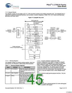
Figure 7-12. Function Mapping Example in a Bank of UDBs
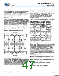
Figure 7-11 shows an example of a 16 UDB array. In addition to
the array core, there are a DSI routing interfaces at the top and
bottom of the array. Other interfaces that are not explicitly shown
include the system interfaces for bus and clock distribution. The
UDB array includes multiple horizontal and vertical routing
channels each comprised of 96 wires. The wire connections to
UDBs, at horizontal/vertical intersection and at the DSI interface
are highly permutable providing efficient automatic routing in
PSoC Creator. Additionally the routing allows wire by wire
segmentation along the vertical and horizontal routing to further
increase routing flexibility and capability.
8-Bit
Timer
16-Bit
PWM
Quadrature Decoder
16-Bit PYRS
UDB
UDB
UDB
UDB
HV
A
HV
B
HV
A
HV
B
UDB
8-Bit
UDB
8-Bit SPI
UDB
UDB
Timer
Logic
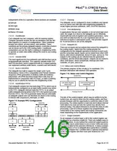
Figure 7-11. Digital System Interface Structure
I2C Slave
UDB
12-Bit SPI
UDB
UDB
UDB
System Connections
HV
B
HV
A
HV
B
HV
A
HV
B
HV
A
HV
B
HV
A
Logic
UDB
UDB
UDB
UDB
UDB
UDB
UDB
UDB
HV
A
HV
B
HV
A
HV
B
UART
12-Bit PWM
UDB
UDB
UDB
UDB
UDB
UDB
UDB
UDB
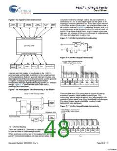
7.4 DSI Routing Interface Description
The DSI routing interface is a continuation of the horizontal and
vertical routing channels at the top and bottom of the UDB array
core. It provides general purpose programmable routing
between device peripherals, including UDBs, I/Os, analog
peripherals, interrupts, DMA and fixed function peripherals.
HV
B
HV
A
HV
B
HV
A
Figure 7-13 illustrates the concept of the digital system
interconnect, which connects the UDB array routing matrix with
other device peripherals. Any digital core or fixed function
peripheral that needs programmable routing is connected to this
interface.
UDB
UDB
UDB
UDB
HV
A
HV
B
HV
A
HV
B
Signals in this category include:
System Connections
Interrupt requests from all digital peripherals in the system.
DMA requests from all digital peripherals in the system.
Digital peripheral data signals that need flexible routing to I/Os.
Digital peripheral data signals that need connections to UDBs.
Connections to the interrupt and DMA controllers.
Connection to I/O pins.
7.3.1 UDB Array Programmable Resources
Figure 7-12 shows an example of how functions are mapped into
a bank of 16 UDBs. The primary programmable resources of the
UDB are two PLDs, one datapath and one status/control register.
These resources are allocated independently, because they
have independently selectable clocks, and therefore unused
blocks are allocated to other unrelated functions.
Connection to analog system digital signals.
Document Number: 001-56955 Rev. *J
Page 47 of 119
[+] Feedback

 CYPRESS [ CYPRESS ]