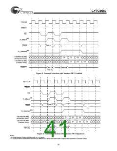
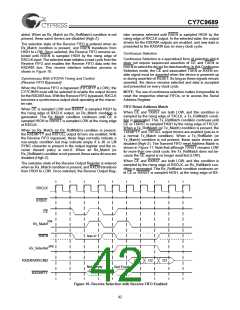
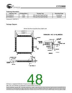
CY7C9689
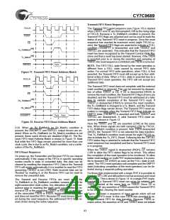
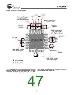
Printed Circuit Board Layout Suggestions
OUTA±
OUTB±
INA±
INB±
Power Supply Bypass
0.01-µF MLC X7R
1206 Chip Cap (4 sites)
Power Supply Bypass
0.01-µF MLC X7R
CURSETB
Resistor
CURSETA
Resistor
Power Supply Bypass
0.01-µF MLC X7R
1206 Chip Cap (2 sites)
RXSC/D
REFCLK
CY7C9689-AC
CY7C9689-AC
Power Supply Bypass
0.01-µF MLC X7R
RESET
Power Supply Bypass
0.01-µF MLC X7R
Via to V plane
DD
Via to V plane
SS
This is a typical printed circuit board layout showing example
placement of power supply bypass components and other
components mounted on the same side as the CY7C9689.
Other layouts, including cases with components mounted on
the reverse side would work as well.
47

 CYPRESS [ CYPRESS ]