CY7C9689
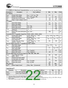
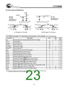
AC Test Loads and Waveforms
5.0V
R1
R2
OUTPUT
V
– 1.3
DD
R1=500 Ω
R2=333 Ω
CL ≤ 10 pF
R =50 Ω
L
C
L
R
L
C
C < 5 pF
L
L
(Includes fixture and
probe capacitance)
(Includes fixture and
probe capacitance)
[17]
[17]
(a) TTLAC Test Load
(b) PECL AC Test Load
V
IHE
3.0V
2.0V
V
V
3.0V
IHE
2.0V
0.8V
80%
80%
Vth=1.5V
Vth=1.5V
< 1 ns
20%
≤ 250 ps
20%
≤ 250 ps
0.8V
0.0V
ILE
V
ILE
< 1 ns
(c) TTLInput Test Waveform
(d) PECL Input Test Waveform
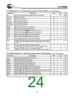
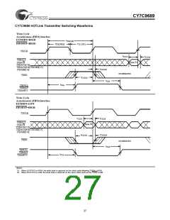
CY7C9689 Transmitter TTL Switching Characteristics, FIFO Enabled Over the Operating Range
Parameter
Description
TXCLK Clock Cycle Frequency With Transmit FIFO Enabled
TXCLK Period
Min.
Max.
Unit
MHz
ns
ns
ns
ns
ns
ns
ns
ns
ns
ns
ns
ns
ns
ns
ns
ns
ns
f
t
t
t
t
t
t
t
t
t
t
t
t
t
t
t
t
t
50
TS
20
6.5
6.5
0.7
0.7
2
TXCLK
TXCLK HIGH Time
TXCPWH
TXCPWL
[16]
TXCLKR
TXCLK LOW Time
[18]
TXCLK Rise Time
5
5
[16]
[18]
TXCLK Fall Time
TXCLKF
TXA
Flag Access Time From TXCLK↑ to Output
15
Transmit Data Set-Up Time to TXCLK↑
4
TXDS
Transmit Data Hold Time from TXCLK↑
1
TXDH
Transmit Enable Set-Up Time to TXCLK↑
4
TXENS
TXENH
TXRSS
TXRSH
TXCES
TXCEH
TXZA
Transmit Enable Hold Time from TXCLK↑
1
Transmit FIFO Reset (TXRST) Set-Up Time to TXCLK↑
Transmit FIFO Reset (TXRST Hold Time from TXCLK↑
Transmit Chip Enable (CE) Set-Up Time to TXCLK↑
Transmit Chip Enable (CE) Hold Time from TXCLK↑
Sample of CE LOW by TXCLK↑, Output High-Z to Active HIGH or LOW
Sample of CE LOW by TXCLK↑ to Output Valid
Sample of CE HIGH by TXCLK↑ to Output in High-Z
4
1
4
1
0
1.5
1.5
20
20
TXOE
TXAZ
Notes:
17. Cypress uses constant current (ATE) load configurations and forcing functions. This figure is for reference only.
18. Input/output rise and fall time is measured between 0.8V and 2.0V
23

 CYPRESS [ CYPRESS ]