CY7C68300B/CY7C68301B
CY7C68320/CY7C68321
8.4.2
MfgCB
Table 8-4. Mfg_load Data Format (continued)
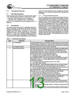
The mfg_load and mfg_read vendor-specific commands will
be passed down through the bulk pipe in the CBWCB portion
of the CBW. The format of this MFGCB is shown below. Byte
0 is a vendor-specific command designator whose value is
configurable and set in the configuration data. Byte 1 must be
0x27 to identify MfgCB. Byte 2–15 are reserved and must be
set to zero.
Byte
Bit(s)
7:0
Function
2
3
4
DD[7:0]
7:0
DD[15:8]
Reserved
7:6
5:0
GPIO Output Enable [5:0]
Reserved
The data transfer length will be determined by the CBW Data
5
6
7:6
Transfer Length specified in bytes
8
through 11
5:0
GPIO Output Data [5:0]
Reserved
(dCBWDataTransferLength) of the CBW. The type/direction of
the command is determined by the direction bit specified in
byte 12, bit 7 (bmCBWFlags) of the CBW.
7:0
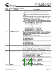
8.4.2.2 Mfg_read
Table 8-3. Example MfgCB
This USB request returns a “snapshot in time” of select AT2LP
input pins. AT2LP input pins not directly associated with USB
operation, can be sampled at any time during Manufacturing
Test Mode operation. See Table 8-5 for an explanation of the
mfg_read data format. The data length shall always be eight
bytes.
Offset MfgCB Byte Description
Bits
7 6 5 4 3 2 1 0
0 0 1 0 0 1 0 0
0
1
0 bVSCBSignature
(set in configuration bytes)
1 bVSCBSubCommand
(hardcoded 0x27)
0 0 1 0 0 1 1 1
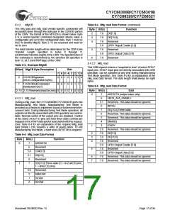
Table 8-5. Mfg_read Data Format
Byte
Bit(s)
7
Data
ARESET# (output value only)
VBUS_ATA_ENABLE
Reserved. This data should be ignored.
INTRQ
2–15 2–15 Reserved (must be zero) 0 0 0 0 0 0 0 0
0
8.4.2.1 Mfg_load
6
During a mfg_load, the CY7C68300B/CY7C68301B goes into
Manufacturing Test Mode. Manufacturing Test Mode is
provided as a means to implement board or system level inter-
connect tests. During Manufacturing Test Mode operation, all
outputs not directly associated with USB operation are control-
lable. Normal control of the output pins are disabled. Control
of the select AT2LP IO pins and their three-state controls are
mapped to the ATAPI data packet associated with this request.
(See Table 8-4 for an explanation of the required Mfg_load
data format.) This requires a write of seven bytes. To exit
Manufacturing Test Mode, a hard reset (RESET#) is required.
5:1
0
1
7
DD[15:0] Three-state
Reserved. This data should be ignored.
Reserved. This data should be ignored.
DMARQ
6
5
4
1
3
IORDY
2:0
7:0
7:0
7:6
5:0
7:6
5:0
7:0
7:0
Reserved. This data should be ignored.
DD[7:0]
2
3
4
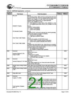
Table 8-4. Mfg_load Data Format
DD[15:8]
Byte
Bit(s)
Function
Reserved
0
7
6
ARESET#
Reserved
CS#[1:0]
DA[2:0]
GPIO Output Enable [5:0]
Reserved
5
5:4
3:1
0
GPIO Output Data [5:0]
Reserved. This data should be ignored.
Reserved. This data should be ignored.
6
7
Reserved
1
7
DD[15:0] Three-state (0 = Hi-Z all DD pins,
1 = drive DD pins).
3:6
2
Reserved
DMACK#
DIOR#
1
0
DIOW#
Document 38-08033 Rev. *D
Page 17 of 36

 CYPRESS [ CYPRESS ]