CY7C68300B/CY7C68301B
CY7C68320/CY7C68321
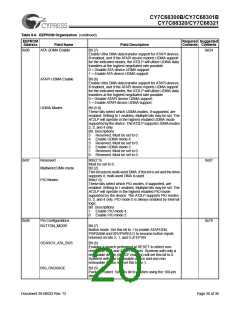
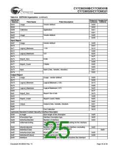
Table 8-6. EEPROM Organization (continued)
EEPROM
Address
Required Suggested
Contents Contents
Field Name
Field Description
ATA_EN
Bit (4)
ATA sharing enable. Allows ATA bus sharing with other host
devices. If ATA_EN=1 the ATA interface will be driven when
VBUS_ATA_ENABLE is LOW. If ATA_EN=0 the ATA
interface will be placed into Hi-Z state whenever
VBUS_ATA_ENABLE is LOW.
‘0’ = ATA signals Hi-Z when VBUS_ATA_ENABLE is LOW.
‘1’ = ATA signals driven when VBUS_ATA_ENABLE is LOW.
DISKRDY Polarity
Bit (3)
DISKRDY active polarity.
‘0’ = Active LOW polarity.
‘1’ = Active HIGH polarity.
HS Indicator Enable
Bit (2)
Enables GPIO2_nHS pin to indicate the current operating
speed of the device (if output is enabled).
‘0’ = Normal GPIO operation.
‘1’ = High-speed indicator enable.
Drive Power Valid Polarity
Drive Power Valid Enable
Bit (1)
Controls the polarity of DRVPWRVLD pin
‘0’ = Active LOW (“connector ground” indication)
‘1’ = Active HIGH (power indication from device)
Bit (0)
Enable for the DRVPWRVLD pin. When this pin is enabled,
the AT2LP will enumerate a removable IDE device (normally
CompactFlash) as the master device.
‘0’ = pin disabled (most systems)
‘1’ = pin enabled (CompactFlash systems)
0x09
0x0A
Reserved
Bits (7:6)
Must be set to zero.
Bits (5:0)
GPIO[5:0] Hi-Z control.
‘0’ = Output enabled (GPIO pin is an output).
‘1’ = Hi-Z (GPIO pin is an input).
0x00
0x00
General Purpose IO Pin
Output Enable
Reserved
Bits (7:6)
Must be set to zero.
General Purpose IO Pin Data Bits (5:0)
If the output enable bit is set, these bits select the value
driven on the GPIO pins.
0x0B
0x0C
Identify Device String Pointer If this value is 00, the Identify Device data will be taken from
0x00
0x00
LUN0
the device. If this string is non-zero, it is used as a pointer to
a 24 byte ASCII (non-Unicode) string in the EEPROM. This
string will be used as the device identifier. This string is used
by many operating systems as the user-visible name for the
device.
Identify Device String Pointer
LUN1
0x0D
0x0E
Delay after reset
Number of 20-ms ticks to wait between RESET and
attempting to access the drive.
0x00
0x00
Reserved
Bits (7:4)
Enable CF UDMA
Bit (3)
‘1’ = Allow UDMA to be used with removable-media devices
‘0’ = UDMA will not be used with removable-media devices
Some CF devices will interfere with UDMA if the UDMA lines
are connected to them. This bit tells the AT2LP if the UDMA
lines are connected to the removable-media device.
Fixed number of logical
units = 2
Bit (2)
If bits 1 and 2 are both 0, the number of logical units will be
determined by searching the ATA and CF buses for devices.
Document 38-08033 Rev. *D
Page 21 of 36

 CYPRESS [ CYPRESS ]