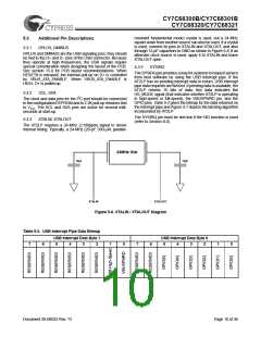
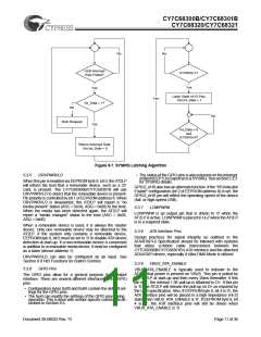
CY7C68300B/CY7C68301B
CY7C68320/CY7C68321
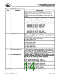
Table 7-1. ATACB Field Descriptions (continued)
Byte
Field Name
Field Description
Bit 1 DeviceSelectionOverride – This bit determines when the device selection
will be performed in relation to the command register write accesses.
0 = Device selection will be performed prior to command register write
accesses
1 = Device selection will be performed following command register write
accesses
Bit 0 TaskFileRead – This bit determines whether or not the taskfile register
data selected in bmATACBRegisterSelect is returned. If this bit is set, the
dCBWDataTransferLength field must be set to 8.
0 = Execute ATACB command and data transfer (if any)
1 = Only read taskfile registers selected in bmATACBRegisterSelect and return
0x00h for all others. The format of the 12 bytes of returned data is as follows:
• Address offset 0x00 (0x3F6) – Alternate Status
• Address offset 0x01 (0x1F1) – Features / Error
• Address offset 0x02 (0x1F2) – Sector Count
• Address offset 0x03 (0x1F3) – Sector Number
• Address offset 0x04 (0x1F4) – Cylinder Low
• Address offset 0x05 (0x1F5) – Cylinder High
• Address offset 0x06 (0x1F6) – Device / Head
• Address offset 0x07 (0x1F7) – Command / Status
3
bmATACBRegisterSelect
This field controls which of the taskfile register read or write accesses occur.
Taskfile read data will always be 8 bytes in length, and unselected register data
will be returned as 0x00. Register accesses occur in sequential order as
outlined below (0 to 7).
Bit 0 (0x3F6) Device Control / Alternate Status
Bit 1 (0x1F1) Features / Error
Bit 2 (0x1F2) Sector Count
Bit 3 (0x1F3) Sector Number
Bit 4 (0x1F4) Cylinder Low
Bit 5 (0x1F5) Cylinder High
Bit 6 (0x1F6) Device / Head
Bit 7 (0x1F7) Command / Status
4
bATACBTransferBlockCount
bATACBTaskFileWriteData
This value indicates the maximum requested block size in 512-byte incre-
ments. This value must be set to the last value used for the “Sectors per block”
in the SET_MULTIPLE_MODE command. Legal values are 0, 1, 2, 4, 8, 16,
32, 64, and 128 where 0 indicates 256 sectors per block. A command failed
status will be returned if an illegal value is used in the ATACB.
5–12
These bytes contain ATA register data used with ATA command or PIO write
operations. Only registers selected in bmATACBRegisterSelect are required to
hold valid data when accessed. The registers are as follows.
ATACB Address Offset 0x05 (0x3F6) – Device Control
ATACB Address Offset 0x06 (0x1F1) – Features
ATACB Address Offset 0x07 (0x1F2) – Sector Count
ATACB Address Offset 0x08 (0x1F3) – Sector Number
ATACB Address Offset 0x09 (0x1F4) – Cylinder Low
ATACB Address Offset 0x0A (0x1F5) – Cylinder High
ATACB Address Offset 0x0B (0x1F6) – Device
ATACB Address Offset 0x0C (0x1F7) – Command
These bytes must be set to 0x00 for ATACB commands.
13–15
Reserved
Document 38-08033 Rev. *D
Page 14 of 36

 CYPRESS [ CYPRESS ]