CY7C68013A, CY7C68014A
CY7C68015A, CY7C68016A
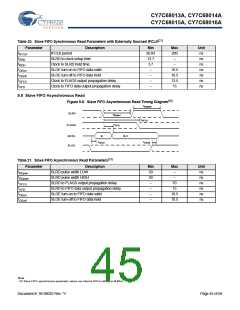
9.13 Slave FIFO Output Enable
Figure 9-14. Slave FIFO Output Enable Timing Diagram[20]
SLOE
t
OEoff
t
OEon
DATA
Table 28. Slave FIFO Output Enable Parameters
Parameter
tOEon
tOEoff
Description
Min
Max
10.5
10.5
Unit
ns
SLOE assert to FIFO DATA output
SLOE deassert to FIFO DATA hold
ns
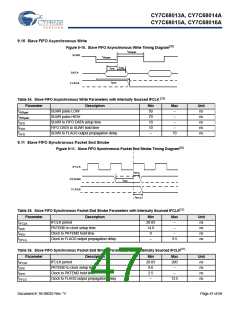
9.14 Slave FIFO Address to Flags/Data
Figure 9-15. Slave FIFO Address to Flags/Data Timing Diagram[20]
FIFOADR [1.0]
t
XFLG
FLAGS
DATA
t
XFD
N
N+1
Table 29. Slave FIFO Address to Flags/Data Parameters
Parameter
tXFLG
tXFD
Description
Min
–
Max
10.7
14.3
Unit
ns
FIFOADR[1:0] to FLAGS output propagation delay
FIFOADR[1:0] to FIFODATA output propagation delay
–
ns
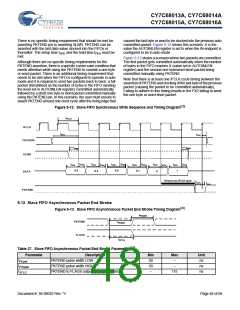
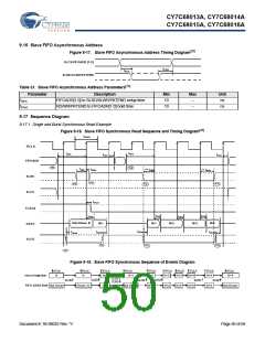
9.15 Slave FIFO Synchronous Address
Figure 9-16. Slave FIFO Synchronous Address Timing Diagram[20]
IFCLK
SLCS/FIFOADR [1:0]
t
t
FAH
SFA
Table 30. Slave FIFO Synchronous Address Parameters [21]
Parameter Description
tIFCLK
tSFA
tFAH
Min
20.83
25
Max
200
–
Unit
ns
Interface clock period
FIFOADR[1:0] to clock setup time
Clock to FIFOADR[1:0] hold time
ns
10
–
ns
Document #: 38-08032 Rev. *V
Page 49 of 66

 CYPRESS [ CYPRESS ]