CY7C68013A, CY7C68014A
CY7C68015A, CY7C68016A
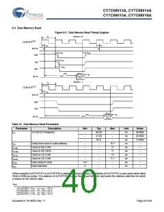
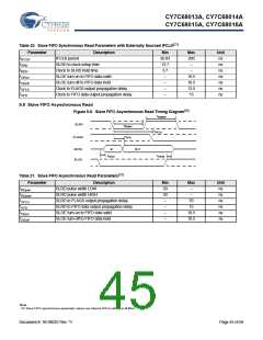
9.1 Slave FIFO Synchronous Read
Figure 9-7. Slave FIFO Synchronous Read Timing Diagram[20]
t
IFCLK
IFCLK
SLRD
t
RDH
t
SRD
t
XFLG
FLAGS
DATA
N+1
N
t
t
XFD
OEon
t
OEoff
SLOE
Table 19. Slave FIFO Synchronous Read Parameters with Internally Sourced IFCLK[21]
Typ
Parameter
tIFCLK
Description
Min
Max
Unit
Min
–
Max
–
IFCLK period
20.83
–
–
ns
ns
ns
ns
ns
ns
ns
ps
ps
%
tSRD
SLRD to clock setup time
18.7
0
–
–
tRDH
Clock to SLRD hold time
–
–
–
tOEon
SLOE turn on to FIFO data valid
SLOE turn off to FIFO data hold
Clock to FLAGS output propagation delay
Clock to FIFO data output propagation delay
IFCLK rise time
–
10.5
10.5
9.5
11
–
–
–
tOEoff
–
–
–
tXFLG
tXFD
–
–
–
–
–
–
tIFCLKR
tIFCLKF
tIFCLKOD
tIFCLKJ
–
–
900
900
51
300
IFCLK fall time
–
–
–
IFCLK Output duty cycle
–
–
49
–
IFCLK jitter peak to peak
–
–
ps
Document #: 38-08032 Rev. *V
Page 44 of 66

 CYPRESS [ CYPRESS ]