CY7C68013A, CY7C68014A
CY7C68015A, CY7C68016A
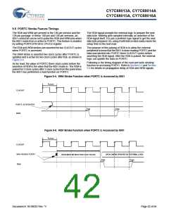
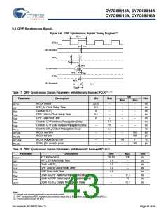
9.5 PORTC Strobe Feature Timings
The RD# and WR# are present in the 100-pin version and the
128-pin package. In these 100-pin and 128-pin versions, an
8051 control bit can be set to pulse the RD# and WR# pins when
the 8051 reads from or writes to PORTC. This feature is enabled
by setting PORTCSTB bit in CPUCS register.
The RD# signal prompts the external logic to prepare the next
data byte. Nothing gets sampled internally on assertion of the
RD# signal itself, it is just a prefetch type signal to get the next
data byte prepared. So, using it with that in mind easily meets the
setup time to the next read.
The RD# and WR# strobes are asserted for two CLKOUT cycles
when PORTC is accessed.
The purpose of this pulsing of RD# is to allow the external
peripheral to know that the 8051 is done reading PORTC and the
data was latched into PORTC three CLKOUT cycles before
asserting the RD# signal. After the RD# is pulsed, the external
logic can update the data on PORTC.
The WR# strobe is asserted two clock cycles after PORTC is
updated and is active for two clock cycles after that, as shown in
Figure 9-4.
Following is the timing diagram of the read and write strobing
function on accessing PORTC. Refer to Section 9.3 and Section
9.4 for details on propagation delay of RD# and WR# signals.
As for read, the value of PORTC three clock cycles before the
assertion of RD# is the value that the 8051 reads in. The RD# is
pulsed for 2 clock cycles after 3 clock cycles from the point when
the 8051 has performed a read function on PORTC.
Figure 9-4. WR# Strobe Function when PORTC is Accessed by 8051
t
CLKOUT
CLKOUT
PORTC IS UPDATED
WR#
t
t
STBL
STBH
Figure 9-5. RD# Strobe Function when PORTC is Accessed by 8051
t
CLKOUT
CLKOUT
8051 READS PORTC
RD#
DATA CAN BE UPDATED BY EXTERNAL LOGIC
DATA MUST BE HELD FOR 3 CLK CYLCES
t
t
STBL
STBH
Document #: 38-08032 Rev. *V
Page 42 of 66

 CYPRESS [ CYPRESS ]