CY7C68013A, CY7C68014A
CY7C68015A, CY7C68016A
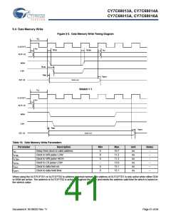
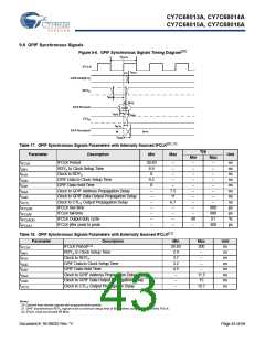
9.4 Data Memory Write
Figure 9-3. Data Memory Write Timing Diagram
t
CL
CLKOUT
A[15..0]
t
AV
t
t
t
STBL
STBH
AV
WR#
CS#
t
SCSL
t
ON1
t
OFF1
data out
D[7..0]
Stretch = 1
t
CL
CLKOUT
A[15..0]
t
AV
WR#
CS#
t
ON1
t
OFF1
data out
D[7..0]
Table 16. Data Memory Write Parameters
Parameter Description
Delay from clock to valid address
Min
Max
10.7
11.2
11.2
13.0
13.1
13.1
Unit
ns
Notes
tAV
0
0
0
–
0
0
–
–
–
–
–
–
tSTBL
tSTBH
tSCSL
tON1
Clock to WR pulse LOW
Clock to WR pulse HIGH
Clock to CS pulse LOW
Clock to data turn-on
ns
ns
ns
ns
tOFF1
Clock to data hold time
ns
When using the AUTPOPTR1 or AUTOPTR2 to address external memory, the address of AUTOPTR1 is only active while either RD#
or WR# are active. The address of AUTOPTR2 is active throughout the cycle and meets the address valid time for which is based on
the stretch value.
Document #: 38-08032 Rev. *V
Page 41 of 66

 CYPRESS [ CYPRESS ]