CY7C68013A, CY7C68014A
CY7C68015A, CY7C68016A
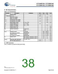
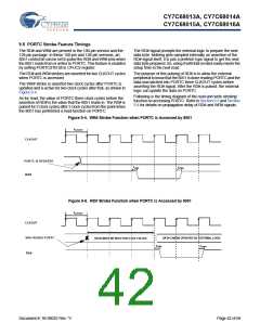
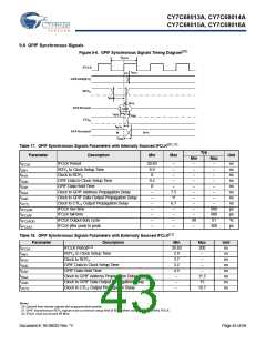
9. AC Electrical Characteristics
9.1 USB Transceiver
USB 2.0 compliant in full speed and high speed modes.
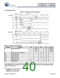
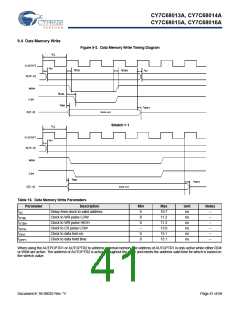
9.2 Program Memory Read
Figure 9-1. Program Memory Read Timing Diagram
t
CL
CLKOUT[17]
t
t
AV
AV
A[15..0]
t
t
STBH
STBL
PSEN#
D[7..0]
[18]
ACC1
t
DH
t
data in
t
SOEL
OE#
CS#
t
SCSL
Table 14. Program Memory Read Parameters
Parameter Description
1/CLKOUT Frequency
Min
–
Typ
Max
–
Unit
ns
ns
ns
ns
ns
ns
ns
ns
ns
ns
Notes
tCL
20.83
48 MHz
–
41.66
–
24 MHz
–
83.2
–
–
12 MHz
tAV
Delay from Clock to Valid Address
Clock to PSEN Low
Clock to PSEN High
Clock to OE Low
0
10.7
8
–
–
–
–
–
–
–
tSTBL
tSTBH
tSOEL
tSCSL
tDSU
tDH
0
–
0
–
8
–
–
11.1
13
–
Clock to CS Low
–
–
Data Setup to Clock
Data Hold Time
9.6
0
–
–
–
Notes
17. CLKOUT is shown with positive polarity.
18. t
is computed from these parameters as follows:
ACC1
ACC1
ACC1
t
t
(24 MHz) = 3*t – t – t
= 106 ns.
= 43 ns.
CL
AV
DSU
DSU
(48 MHz) = 3*t – t – t
CL
AV
Document #: 38-08032 Rev. *V
Page 39 of 66

 CYPRESS [ CYPRESS ]