FOR
FOR
CY7C63411/12/13
CY7C63511/12/13
CY7C63612/13
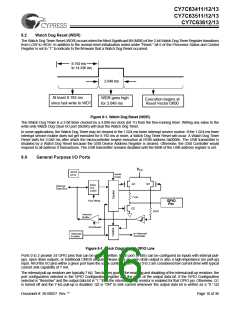
provides “HIGH” source current when the GPIO port is configured for CMOS outputs and the output data bit is written as a “1”.
Q2 and Q3 are sized to sink and source, respectively, roughly the same amount of current to support traditional CMOS outputs
with symmetric drive.
P0[7]
P1[7]
P0[6]
P1[6]
P0[5]
P0[4]
P0[3]
P0[2]
P0[1]
P1[1]
P0[0]
P1[0]
P1[5]
P1[4]
P1[3]
P1[2]
Figure 9-2. Port 1 Data 0x01h (read/write)
P2[7]
P3[7]
P2[6]
P3[6]
P2[5]
P2[4]
P2[3]
P2[2]
P2[1]
P3[1]
P2[0]
P3[0]
Figure 9-3. Port 2 Data 0x02h (read/write)
P3[5]
P3[4]
P3[3]
P3[2]
Figure 9-4. Port 3 Data 0x03h (read/write)
Low current outputs
High current outputs
0.2 mA to 1.0 mA typical
3.2 mA to 16 mA typical
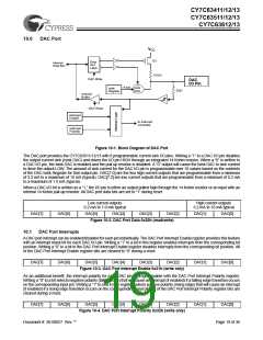
DAC[7]
DAC[6]
DAC[5]
DAC[4]
DAC[3]
DAC[2]
DAC[1]
DAC[0]
Figure 9-5. DAC Port Data 0x30h (read/write)
Port 3 has eight GPIO pins. Port 3 (8 bits) can be configured as inputs with internal pull-ups, open drain outputs, or traditional
CMOS outputs. An open drain output is also a high-impedance input. Port 3 offers high current drive with a typical current sink
capability of 12 mA. The internal pull-up resistors are typically 7 kΩ.
Note: Special care should be exercised with any unused GPIO data bits. An unused GPIO data bit, either a pin on the chip or a
port bit that is not bonded on a particular package, must not be left floating when the device enters the suspend state. If a GPIO
data bit is left floating, the leakage current caused by the floating bit may violate the suspend current limitation specified by the
USB Specification. If a ‘1’ is written to the unused data bit and the port is configured with open drain outputs, the unused data bit
will be in an indeterminate state. Therefore, if an unused port bit is programmed in open-drain mode, it must be written with a ‘0.’
Notice that the CY7C63612/13 will always require that data bits P1[7:4], P2[7:0], P3[3:0] and DAC[7:0] be written with a ‘0.’
During reset, all of the GPIO pins are set to output “1” (input) with the internal pull-up enabled. In this state, a “1” will always be
read on that GPIO pin unless an external current sink drives the output to a “0” state. Writing a “0” to a GPIO pin enables the
output current sink to ground (LOW) and disables the internal pull-up for that pin.
9.1
GPIO Interrupt Enable Ports
During a reset, GPIO interrupts are disabled by clearing all of the GPIO interrupt enable ports. Writing a “1” to a GPIO Interrupt
Enable bit enables GPIO interrupts from the corresponding input pin.
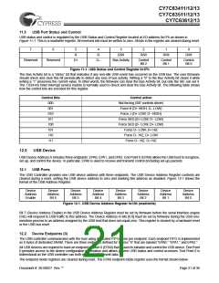
P0[7]
P1[7]
P2[7]
P3[7]
P0[6]
P1[6]
P2[6]
P3[6]
P0[5]
P0[4]
P0[3]
P0[2]
P0[1]
P1[1]
P2[1]
P3[1]
P0[0]
P1[0]
P2[0]
P3[0]
Figure 9-6. Port 0 Interrupt Enable 0x04h (write only)
P1[5]
P1[4]
P1[3]
P1[2]
Figure 9-7. Port 1 Interrupt Enable 0x05h (write only)
P2[5]
P2[4]
P2[3]
P2[2]
Figure 9-8. Port 2 Interrupt Enable 0x06h (write only)
P3[5]
P3[4]
P3[3]
P3[2]
Figure 9-9. Port 3 Interrupt Enable 0x07h (write only)
Document #: 38-08027 Rev. **
Page 17 of 36

 CYPRESS [ CYPRESS ]