FOR
FOR
CY7C63411/12/13
CY7C63511/12/13
CY7C63612/13
8.2
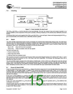
Watch Dog Reset (WDR)
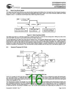
The Watch Dog Timer Reset (WDR) occurs when the Most Significant Bit (MSB) of the 2-bit Watch Dog Timer Register transitions
from LOW to HIGH. In addition to the normal reset initialization noted under “Reset,” bit 6 of the Processor Status and Control
Register is set to “1” to indicate to the firmware that a Watch Dog Reset occurred.
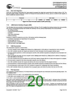
8.192 ms
to 14.336 ms
2.048 ms
At least 8.192 ms
WDR goes high
for 2.048 ms
Execution begins at
Reset Vector 0X00
since last write to WDT
Figure 8-1. Watch Dog Reset (WDR)
The Watch Dog Timer is a 2-bit timer clocked by a 4.096-ms clock (bit 11) from the free-running timer. Writing any value to the
write-only Watch Dog Clear I/O port (0x26h) will clear the Watch Dog Timer.
In some applications, the Watch Dog Timer may be cleared in the 1.024-ms timer interrupt service routine. If the 1.024-ms timer
interrupt service routine does not get executed for 8.192 ms or more, a Watch Dog Timer Reset will occur. A Watch Dog Timer
Reset lasts for 2.048 ms after which the microcontroller begins execution at ROM address 0x0000h. The USB transmitter is
disabled by a Watch Dog Reset because the USB Device Address Register is cleared. Otherwise, the USB Controller would
respond to all address 0 transactions. The USB transmitter remains disabled until the MSB of the USB address register is set.
9.0
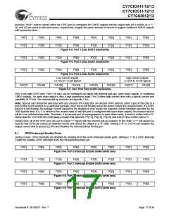
General Purpose I/O Ports
VCC
GPIO
CFG
mode
2 bits
Q3
Q1
Data
Out
Latch
Internal
Data Bus
7 kΩ
Port Write
GPIO
Pin
Q2
ESD
Internal
Buffer
Port Read
to Interrupt
Controller
Interrupt
Enable
Figure 9-1. Block Diagram of a GPIO Line
Ports 0 to 2 provide 24 GPIO pins that can be read or written. Each port (8 bits) can be configured as inputs with internal pull-
ups, open drain outputs, or traditional CMOS outputs. Please note an open drain output is also a high-impedance (no pull-up)
input. All of the I/O pins within a given port have the same configuration. Ports 0 to 2 are considered low current drive with typical
current sink capability of 7 mA.
The internal pull-up resistors are typically 7 kΩ. Two factors govern the enabling and disabling of the internal pull-up resistors: the
port configuration selected in the GPIO Configuration register and the state of the output data bit. If the GPIO Configuration
selected is “Resistive” and the output data bit is “1,” then the internal pull-up resistor is enabled for that GPIO pin. Otherwise, Q1
is turned off and the 7-kΩ pull-up is disabled. Q2 is “ON” to sink current whenever the output data bit is written as a “0.” Q3
Document #: 38-08027 Rev. **
Page 16 of 36

 CYPRESS [ CYPRESS ]