FOR
FOR
CY7C63411/12/13
CY7C63511/12/13
CY7C63612/13
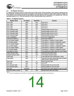
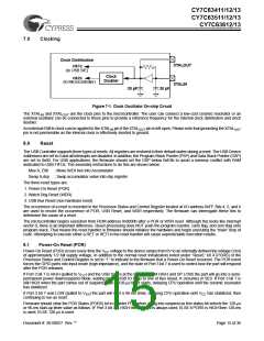
6.3
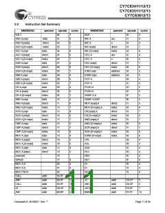
I/O Register Summary
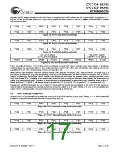
I/O registers are accessed via the I/O Read (IORD) and I/O Write (IOWR, IOWX) instructions. IORD reads the selected port into
the accumulator. IOWR writes data from the accumulator to the selected port. Indexed I/O Write (IOWX) adds the contents of X
to the address in the instruction to form the port address and writes data from the accumulator to the specified port. Note that
specifying address 0 (e.g., IOWX 0h) means the I/O port is selected solely by the contents of X.
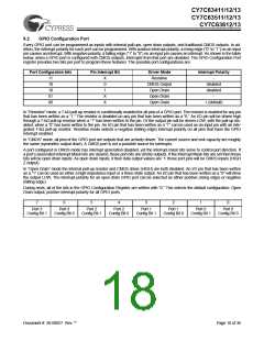
Table 6-1. I/O Register Summary
Register Name
Port 0 Data
I/O Address
0x00
0x01
0x02
0x03
0x04
0x05
0x06
0x07
0x08
0x10
0x11
Read/Write
R/W
R/W
R/W
R/W
W
Function
GPIO Port 0
GPIO Port 1
GPIO Port 2
GPIO Port 3
Port 1 Data
Port 2 Data
Port 3 Data
Port 0 Interrupt Enable
Port 1 Interrupt Enable
Port 2 Interrupt Enable
Port 3 Interrupt Enable
GPIO Configuration
USB Device Address A
EP A0 Counter Register
EP A0 Mode Register
EP A1 Counter Register
EP A1 Mode Register
EP A2 Counter Register
EP A2 Mode Register
USB Status & Control
Global Interrupt Enable
Endpoint Interrupt Enable
Timer (LSB)
Interrupt enable for pins in Port 0
W
Interrupt enable for pins in Port 1
W
Interrupt enable for pins in Port 2
W
Interrupt enable for pins in Port 3
R/W
R/W
R/W
R/W
R/W
R/C
R/W
R/C
R/W
R/W
R/W
R
GPIO Ports Configurations
USB Device Address A
USB Address A, Endpoint 0 counter register
USB Address A, Endpoint 0 configuration register
USB Address A, Endpoint 1 counter register
USB Address A, Endpoint 1 configuration register
USB Address A, Endpoint 2 counter register
USB Address A, Endpoint 2 configuration register
USB upstream port traffic status and control register
Global interrupt enable register
0x12
0x13
0x14
0x15
0x16
0x1F
0x20
0x21
0x24
0x25
USB endpoint interrupt enables
Lower eight bits of free-running timer (1 MHz)
Timer (MSB)
R
Upper four bits of free-running timer that are latched
when the lower eight bits are read.
WDR Clear
0x26
0x30
W
R/W
W
Watch Dog Reset clear
DAC I/O[2]
Interrupt enable for each DAC pin[2]
Interrupt polarity for each DAC pin[2]
One four bit sink current register for each DAC pin[2]
Microprocessor status and control
DAC Data
DAC Interrupt Enable
DAC Interrupt Polarity
DAC Isink
0x31
0x32
W
0x38-0x3F
0xFF
W
Processor Status & Control
R/W
Note:
2. DAC I/O Port not bonded out on CY7C63612/13. See note on page 17 for firmware code needed for unused GPIO pins.
Document #: 38-08027 Rev. **
Page 14 of 36

 CYPRESS [ CYPRESS ]