FOR
FOR
CY7C63411/12/13
CY7C63511/12/13
CY7C63612/13
11.3
USB Port Status and Control
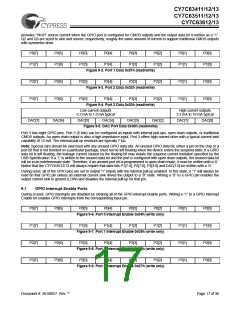
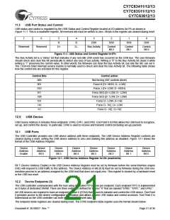
USB status and control is regulated by the USB Status and Control Register located at I/O address 0x1Fh as shown in
Figure 11-1. This is a read/write register. All reserved bits must be written to zero. All bits in the register are cleared during reset.
7
6
5
R
4
R
3
2
1
0
R/W
R/W
R/W
R/W
Reserved
Reserved
D+
D–
Bus Activity
Control
Bit 2
Control
Bit 1
Control
Bit 0
Figure 11-1. USB Status and Control Register 0x1Fh
The Bus Activity bit is a “sticky” bit that indicates if any non-idle USB event has occurred on the USB bus. The user firmware
should check and clear this bit periodically to detect any loss of bus activity. Writing a “0” to the Bus Activity bit clears it while
writing a “1” preserves the current value. In other words, the firmware can clear the Bus Activity bit, but only the SIE can set it.
The 1.024-ms timer interrupt service routine is normally used to check and clear the Bus Activity bit. The following table shows
how the control bits are encoded for this register.
Control Bits
000
Control action
Not forcing (SIE controls driver)
Force K (D+ HIGH, D– LOW)
Force J (D+ LOW, D– HIGH)
Force SE0 (D+ LOW, D– LOW)
Force SE0 (D− LOW, D+ LOW)
Force D− LOW, D+ HiZ
001
010
011
100
101
110
Force D− HiZ, D+ LOW
111
Force D− HiZ, D+ HiZ
12.0
USB Device
USB Device Address A includes three endpoints: EPA0, EPA1, and EPA2. End Point 0 (EPA0) allows the USB host to recognize,
set up, and control the device. In particular, EPA0 is used to receive and transmit control (including set-up) packets.
12.1
USB Ports
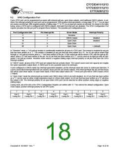
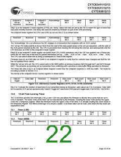
The USB Controller provides one USB device address with three endpoints. The USB Device Address Register contents are
cleared during a reset, setting the USB device address to zero and marking this address as disabled. Figure 12-1 shows the
format of the USB Address Register.
Device
Address
Enable
Device
Address
Bit 6
Device
Address
Bit 5
Device
Address
Bit 4
Device
Address
Bit 3
Device
Address
Bit 2
Device
Address
Bit 1
Device
Address
Bit 0
Figure 12-1. USB Device Address Register 0x10h (read/write)
Bit 7 (Device Address Enable) in the USB Device Address Register must be set by firmware before the serial interface engine
(SIE) will respond to USB traffic to this address. The Device Address in bits [6:0] must be set by firmware during the USB enu-
meration process to an address assigned by the USB host that does not equal zero. This register is cleared by a hardware reset
or the USB bus reset.
12.2
Device Endpoints (3)
The USB controller communicates with the host using dedicated FIFOs, one per endpoint. Each endpoint FIFO is implemented
as 8 bytes of dedicated SRAM. There are three endpoints defined for Device “A” that are labeled “EPA0,” “EPA1,” and EPA2.”
All USB devices are required to have an endpoint number 0 (EPA0) that is used to initialize and control the USB device. End Point
0 provides access to the device configuration information and allows generic USB status and control accesses. End Point 0 is
bidirectional as the USB controller can both receive and transmit data.
The endpoint mode registers are cleared during reset. The EPA0 endpoint mode register uses the format shown below:
Document #: 38-08027 Rev. **
Page 21 of 36

 CYPRESS [ CYPRESS ]