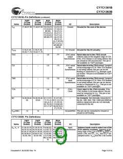
CY7C1361B
CY7C1363B
9-Mbit (256K x 36/512K x 18)
Flow-Through SRAM
Features
Functional Description[1]
• Supports 133-MHz bus operations
• 256K X 36/512K X 18 common I/O
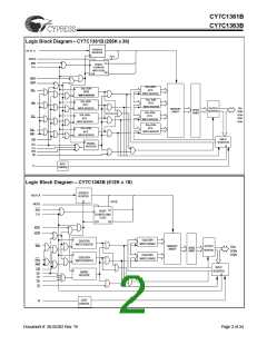
The CY7C1361B/CY7C1363B is a 3.3V, 256K x 36 and 512K
x 18 Synchronous Flow through SRAMs, respectively
designed to interface with high-speed microprocessors with
minimum glue logic. Maximum access delay from clock rise is
6.5 ns (133-MHz version). A 2-bit on-chip counter captures the
first address in a burst and increments the address automati-
cally for the rest of the burst access. All synchronous inputs
are gated by registers controlled by a positive-edge-triggered
Clock Input (CLK). The synchronous inputs include all
• 3.3V –5% and +10% core power supply (VDD
)
• 2.5V or 3.3V I/O supply (VDDQ
• Fast clock-to-output times
— 6.5 ns (133-MHz version)
)
— 7.5 ns (117-MHz version)
— 8.5 ns (100-MHz version)
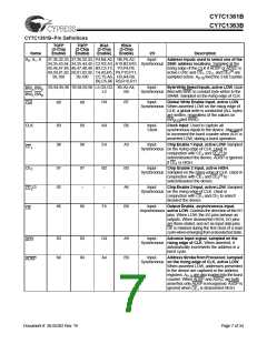
addresses, all data inputs, address-pipelining Chip Enable
[2]
(
), depth-expansion Chip Enables (CE and
), Burst
CE3
• Provide high-performance 2-1-1-1 access rate
CE1
2
Control inputs (
,
,
), Write Enables
(
ADV
BWx
• User-selectable burst counter supporting Intel
and
,
ADSC ADSP
Pentium interleaved or linear burst sequences
), and Global Write (
BWE
). Asynchronous
GW
and
inputs
(
)
and the ZZ pin
OE
.
include the Output Enable
• Separate processor and controller address strobes
• Synchronous self-timed write
The CY7C1361B/CY7C1363B allows either interleaved or
linear burst sequences, selected by the MODE input pin. A
HIGH selects an interleaved burst sequence, while a LOW
selects a linear burst sequence. Burst accesses can be
initiated with the Processor Address Strobe (ADSP) or the
cache Controller Address Strobe (ADSC) inputs. Address
advancement is controlled by the Address Advancement
(ADV) input.
• Asynchronous output enable
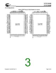
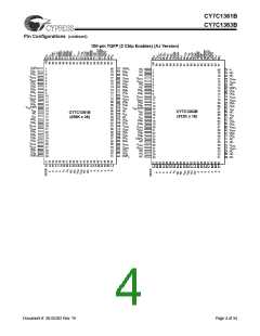
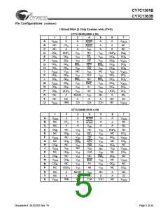
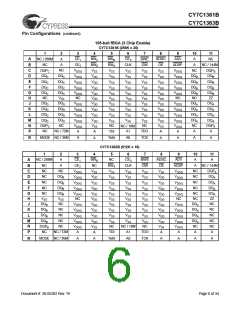
• Offered in JEDEC-standard 100-pin TQFP, 119-ball BGA
and 165-ball fBGA packages
— Both 2 and 3 Chip Enable Options for TQFP
• JTAG boundary scan for BGA and fBGA packages
• “ZZ” Sleep Mode option
Addresses and chip enables are registered at rising edge of
clock when either Address Strobe Processor (
) or
ADSP
Address Strobe Controller (
) are active. Subsequent
ADSC
burst addresses can be internally generated as controlled by
the Advance pin ( ).
ADV
The CY7C1361B/CY7C1363B operates from a +3.3V core
power supply while all outputs may operate with either a +2.5
or +3.3V supply. All inputs and outputs are JEDEC-standard
JESD8-5-compatible.
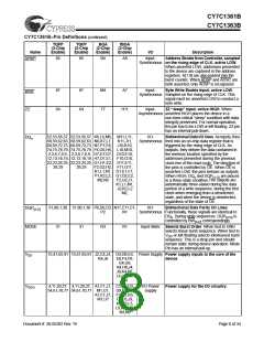
Selection Guide
133 MHz
117 MHz
7.5
100 MHz
8.5
Unit
ns
mA
mA
Maximum Access Time
Maximum Operating Current
Maximum CMOS Standby Current
6.5
250
30
220
30
180
30
Notes:
1. For best–practices recommendations, please refer to the Cypress application note System Design Guidelines on www.cypress.com.
2. CE is for A version of TQFP (3 Chip Enable Option) and 165 fBGA package only. 119 BGA is offered only in 2 Chip Enable.
3
Cypress Semiconductor Corporation
•
3901 North First Street
•
San Jose, CA 95134
•
408-943-2600
Document #: 38-05302 Rev. *B
Revised April 20, 2004

 CYPRESS [ CYPRESS ]