CY7B923
CY7B933
table. If SC/D is LOW, the data inputs are converted using the Data
code table. If a byte time passes with the inputs disabled, the En-
coder will output a Special Character Comma K28.5 (or SYNC) that
will maintain link synchronization. SVS input forces the transmis-
sion of a specified Violation symbol to allow the user to check error
handling system logic in the controller or for proprietary applications.
pulse stream will insure correct data transfers between asynchro-
nous FIFOs and the transmitter input latch with no external logic.
Test Logic
Test logic includes the initialization and control for the Built-In
Self-Test (BIST) generator, the multiplexer for Test mode clock
distribution, and control logic to properly select the data encod-
ing. Test logic is discussed in more detail in the CY7B923
HOTLink Transmitter Operating Mode Description.
The 8B/10B coding function of the Encoder can be bypassed
for systems that include an external coder or scrambler func-
tion as part of the controller. This bypass is controlled by set-
ting the MODE select pin HIGH. When in bypass mode, D
(note that bit order is specified in the Fibre Channel 8B/10B code)
a−j
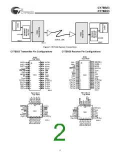
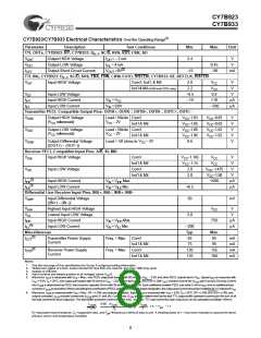
CY7B933 HOTLink Receiver Block Diagram
Description
become the ten inputs to the Shifter, with D being the first bit to be
a
shifted out.
Serial Data Inputs
Shifter
Two pairs of differential line receivers are the inputs for the
serial data stream. INA± or INB± can be selected with the A/B
input. INA± is selected with A/B HIGHand INB± is selected with A/B
LOW. The threshold of A/B is compatiblewith the ECL 100Ksignals
from PECL fiber optic interface modules. TTL logic elements can be
used to select the A or B inputs by adding a resistor pull-up to the
TTL driver connected to A/B. The differential threshold of INA± and
INB± will accommodate wire interconnect with filtering losses or
The Shifter accepts parallel data from the Encoder once each
byte time and shifts it to the serial interface output buffers using
a PLL multiplied bit clock that runs at ten (10) times the byte
clock rate. Timing for the parallel transfer is controlled by the
counter included in the Clock Generator and is not affected by
signal levels or timing at the input pins.
OutA, OutB, OutC
transmission line attenuation greater than 20 db (V
> 50 mv) or
DIF
can be directly connected to fiber optic interface modules (any ECL
logic family, not limited to ECL 100K). The common mode tolerance
will accommodate a wide range of signal termination voltages. The
The serial interface PECL output buffers (ECL100K referenced
to +5V) are the drivers for the serial media. They are all con-
nected to the Shifter and contain the same serial data. Two of
the output pairs (OUTA± and OUTB±) are controllable by the
FOTO input and can be disabled by the system controller to force a
logical zero (i.e., “light off”) at the outputs. The third output pair
(OUTC±) is not affected by FOTO and will supply a continuous data
stream suitable for loop-back testing of the subsystem.
highest HIGH input that can be tolerated is V = V , and the low-
IN
CC
est LOW input that can be interpreted correctly is V = GND+2.0V.
IN
PECL-TTL Translator
The function of the INB(INB+) input and the SI(INB−) input is
defined by the connections on the SO output pin. If the
PECL/TTL translator function is not required, the SO output is
wired to VCC. A sensor circuit will detect this connection and
cause the inputs to become INB± (a differential line-receiver seri-
al-data input). If the PECL/TTL translator function is required, the
SOoutputisconnectedtoitsnormal TTLload(typicallyoneor more
TTL inputs, but nopull-upresistor) and the INB+input becomesINB
(single-ended ECL 100K, serial data input) and the INB− input be-
comes SI (single-ended, ECL 100K status input).
OUTA± and OUTB± will respond to FOTO input changes within a
few bit times. However, since FOTO is not synchronized with the
transmitter data stream, the outputs will be forced off or turned on
at arbitrary points in a transmitted byte. This function is intended to
augment anexternallasersafetycontroller andasanaidfor Receiv-
er PLL testing.
In wire-based systems, control of the outputs may not be re-
quired, and FOTO can be strapped LOW. The three outputs
are intended to add system and architectural flexibility by of-
fering identical serial bit streams with separate interfaces for
redundant connections or for multiple destinations. Unneeded
outputs can be wired to VCC to disable and power down the un-
used output circuitry.
This positive-referenced PECL-to-TTL translator is provided to
eliminate external logic between an PECL fiber-optic interface
module “carrier detect” output and the TTL input in the control
logic. The input threshold is compatible with ECL 100K levels
(+5V referenced). It can also be used as part of the link status
indication logic for wire connected systems.
Clock Generator
The clock generator is an embedded phase-locked loop (PLL)
that takes a byte-rate reference clock (CKW) and multiplies it
by ten (10) to create a bit rate clock for driving the serial shifter.
The byte rate reference comes from CKW, the rising edge of
which clocks data into the Input register. This clock must be a
crystal referenced pulse stream that has a frequency between
the minimum and maximum specified for the HOTLink Trans-
mitter/Receiver pair. Signals controlled by this block form the
bit clock and the timing signals that control internal data trans-
fers between the Input register and the Shifter.
Clock Synchronization
The Clock Synchronization function is performed by an em-
bedded phase-locked loop (PLL) that tracks the frequency of
the incoming bit stream and aligns the phase of its internal bit
rate clock to the serial data transitions. This block contains the
logic to transfer the data from the Shifter to the Decode register
once every byte. The counter that controls this transfer is ini-
tialized by the Framer logic. CKR is a buffered output derived
from the bit counter used to control the Decode register and
the output register transfers.
The read pulse (RP) is derived from the feedback counter used in
the PLL multiplier. It is a byte-rate pulse stream with the proper
phase and pulse widths to allow transfer of data from an asynchro-
nous FIFO. Pulse width is independent of CKW duty cycle, since
proper phase and duty cycle is maintained by the PLL. The RP
Clock output logic is designed so that when reframing causes
the counter sequence to be interrupted, the period and pulse
width of CKR will never be less than normal. Reframing may
stretch the period of CKR by up to 90%, and either CKR Pulse
Width HIGH or Pulse Width LOW may be stretched, depending
on when reframe occurs.
6

 CYPRESS [ CYPRESS ]