CY7B923
CY7B933
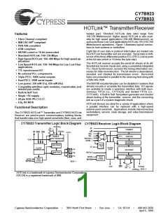
CY7B923 HOTLink Transmitter (continued)
Name
I/O
Description
OUTA±
OUTB±
OUTC±
PECL Out Differential Serial Data Outputs. These PECL 100K outputs (+5V referenced) are capable of driving
terminated transmission lines or commercial fiber optic transmitter modules. Unused pairs of outputs
can be wired to V to reduce power if the output is not required. OUTA± and OUTB± are controlled by the
CC
level on FOTO, and will remain at their “logical zero” states when FOTO is asserted. OUTC± is unaffected
by the level on FOTO. (OUTA+ and OUTB+ are used as a differential test clock input while in Test mode, i.e.,
MODE=UNCONNECTED or forced to V /2.)
CC
MODE
3-Level In Encoder Mode Select. The level on MODE determines the encoding method to be used. When
wired to GND, MODE selects 8B/10B encoding. When wired to V , data inputs bypass the encoder
CC
and the bit pattern on D goes directly to the shifter. When left floating (internal resistors hold the input at
a-j
V
/2) the internal bit-clock generator is disabled and OUTA+/OUTB+ become the differential bit clock to be
CC
used for factory test. In typical applications MODE is wired to V or GND.
CC
BISTEN
TTL In
Built-In Self-Test Enable. When BISTEN is LOW and ENA and ENN are HIGH, the transmitter sends an
alternating 1−0 pattern (D10.2 or D21.5). When either ENA or ENN is set LOW and BISTEN is LOW, the
transmitter begins a repeating test sequence that allows the Transmitter and Receiver to work together to test
the function of the entire link. In normal use this input is held HIGH or wired to V . The BIST generator is
CC
a free-running pattern generator that need not be initialized, but if required, the BIST sequence can be
initialized by momentarily asserting SVS while BISTEN is LOW. BISTEN has the same timing as D
.
0−7
RP
TTL Out
Read Pulse. RP is a 60% LOW duty-cycle byte-rate pulse train suitable for the read pulse in CY7C42X
FIFOs. The frequency on RP is the same as CKW when enabled by ENA, and duty cycle is independent of
the CKW duty cycle. Pulse widths are set by logic internal to the transmitter. In BIST mode, RP will remain
HIGH for all but the last byte of a test loop. RP will pulse LOW one byte time per BIST loop.
V
V
Power for output drivers.
Power for internal circuitry.
Ground.
CCN
CCQ
GND
CY7B933 HOTLink Receiver
Name
I/O
Description
Q Parallel Data Output. Q contain the most recently received data. These outputs change synchro-
0−7
Q
TTL Out
0−7
0−7
(Q
)
nously with CKR. When MODE is HIGH, Q
become Q
respectively.
b − h
0, 1, ...7
b, c,...h
SC/D(Q )
TTL Out
TTL Out
Special Character/Data Select. SC/D indicates the context of received data. HIGH indicates a Control
(Special Character) code, LOW indicates a Data character. When MODE is HIGH (placing the receiver in
a
Unencoded mode), SC/D acts as the Q output. SC/D has the same timing as Q
.
a
0−7
RVS (Q)
Received Violation Symbol. A HIGH on RVS indicates that a code rule violation has been detected
in the received data stream. A LOW shows that no error has been detected. In BIST mode, a LOW
on RVS indicates correct operation of the Transmitter, Receiver, and link on a byte-by-byte basis.
j
When MODE is HIGH (placing the receiver in Unencoded mode), RVS acts as the Q output. RVShas
j
the same timing as Q
.
0−7
RDY
TTL Out
Data Output Ready. A LOW pulse on RDY indicates that new data has been received and is ready to be
delivered. A missing pulse on RDY shows that the received data is the Null character (normally inserted by
the transmitter as a pad between data inputs). In BIST mode RDY will remain LOW for all but the last byte
of a test loop and will pulse HIGH one byte time per BIST loop.
CKR
A/B
TTL Out
PECL in
Clock Read. This byte rate clock output is phase and frequency aligned to the incoming serial data
stream. RDY, Q , SC/D, and RVS all switch synchronously with the rising edge of this output.
0−7
Serial Data Input Select. This PECL 100K (+5V referenced) input selects INA or INB as the active
data input. If A/B is HIGH, INA is connected to the shifter and signals connected to INA will be decoded. If
A/B is LOW INB is selected.
INA±
Diff In
Serial Data Input A. The differential signal at the receiver end of the communication link may be
connected to the differential input pairs INA± or INB±. Either the INA pair or the INB pair can be used as
the main data input and the other can be used as a loopback channel or as an alternative data input selected
by the state of A/B.
4

 CYPRESS [ CYPRESS ]