CY7B923
CY7B933
Maximum Ratings
(Above which the useful life may be impaired. For user guide-
lines, not tested.)
Static Discharge Voltage ........................................... >4001V
(per MIL−STD−883, Method 3015)
Storage Temperature......................................−65°C to +150°C
Latch-Up Current..................................................... >200 mA
Ambient Temperature with
Power Applied..................................................−55°C to +125°C
Operating Range
Ambient
Supply Voltage to Ground Potential................. −0.5V to +7.0V
DC Input Voltage ................................................ −0.5V to +7.0V
Output Current into TTL Outputs (LOW)......................30 mA
Output Current into PECL outputs (HIGH)...................−50 mA
Range
Commercial
Industrial
Military
Temperature
0°C to +70°C
−40°C to +85°C
V
CC
5V ± 10%
5V ± 10%
5V ± 10%
−55°C to +125°C
Case Temperature
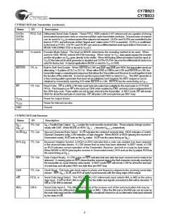
Pin Descriptions
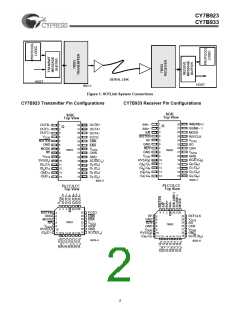
CY7B923 HOTLink Transmitter
Name
I/O
Description
D
(D
TTL In
Parallel Data Input. Data is clocked into the Transmitter on the rising edge of CKW if ENA is LOW
(or on the next rising CKW with ENN LOW). If ENA and ENN are HIGH, a Null character (K28.5) is
0−7
)
b − h
sent. When MODE is HIGH, D
become D
respectively.
0, 1, ...7
b, c,...h
SC/D (D ) TTL In
Special Character/Data Select. A HIGH on SC/D when CKW rises causes the transmitter to encode
the pattern on D as a control code (Special Character), while a LOW causes the data to be coded
a
0−7
using the 8B/10B data alphabet. When MODE is HIGH, SC/D (D ) acts as D input. SC/D has the
a
a
same timing as D
.
0−7
SVS
TTL In
TTL In
TTL In
Send Violation Symbol. If SVS is HIGH when CKW rises, a Violation symbol is encoded and sent
while the data on the parallel inputs is ignored. If SVS is LOW, the state of D and SC/D determines
the code sent. In normal or test mode, this pin overrides the BIST generator and forces the trans-
mission of a Violation code. When MODE is HIGH (placing the transmitter in unencoded mode),
(D )
j
0−7
SVS (D ) acts as the D input. SVS has the same timing as D .
j
j
0−7
ENA
ENN
Enable Parallel Data. If ENA is LOW on the rising edge of CKW, the data is loaded, encoded, and
sent. If ENA and ENN are HIGH, the data inputs are ignored and the Transmitter will insert a Null
character (K28.5) to fill the space between user data. ENA may be held HIGH/LOW continuously or
it may be pulsed with each data byte to be sent. If ENA is being used for data control, ENN will
normally be strapped HIGH, but can be used for BIST function control.
Enable Next Parallel Data. If ENN is LOW, the data appearing on D
at the next rising edge of
0−7
CKW is loaded, encoded, and sent. If ENA and ENN are HIGH, the data appearing on D
at the
0−7
next rising edge of CKW will be ignored and the Transmitter will insert a Null character to fill the space
between user data. ENN may be held HIGH/LOW continuously or it may be pulsed with each data
byte sent. If ENN is being used for data control, ENA will normally be strapped HIGH, but can be
used for BIST function control.
CKW
TTL In
TTL In
Clock Write. CKW is both the clock frequency reference for the multiplying PLL that generates the
high−speed transmit clock, and the byte rate write signal that synchronizes the parallel data input.
CKW must be connected to a crystal controlled time base that runs within the specified frequency
range of the Transmitter and Receiver.
FOTO
Fiber Optic Transmitter Off. FOTO determines the function of two of the three PECL transmitter
output pairs. If FOTO is LOW, the data encoded by the Transmitter will appear at the outputs con-
tinuously. If FOTO is HIGH, OUTA± and OUTB± are forced to their “logic zero” state (OUT+ = LOW
and OUT− = HIGH), causing a fiber optic transmit module to extinguish its light output. OUTC is
unaffected by the level on FOTO, and can be used as a loop-back signal source for board-level
diagnostic testing.
3

 CYPRESS [ CYPRESS ]