CY7B923
CY7B933
[1]
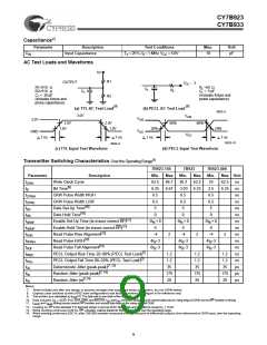
CY7B923/CY7B933 Electrical Characteristics Over the Operating Range
Parameter
Description
Test Conditions
Min.
2.4
Max.
Unit
TTL OUTs, CY7B923: RP; CY7B933: Q , SC/D, RVS, RDY, CKR, SO
0−7
V
Output HIGH Voltage
I
I
= − 2 mA
V
V
OHT
OH
OL
V
Output LOW Voltage
= 4 mA
0.45
OLT
[2]
I
Output Short Circuit Current
V
=0V
−15
−90
mA
OST
OUT
TTL INs, CY7B923: D , SC/D, SVS, ENA, ENN, CKW, FOTO, BISTEN; CY7B933: RF, REFCLK, BISTEN
0−7
V
Input HIGH Voltage
Com’l, Ind’l, & Mil
2.0
2.2
V
V
V
V
IHT
CC
CC
Ind’l & Mil (CKWandFOTO,only)
V
Input LOW Voltage
Input HIGH Current
Input LOW Current
−0.5
−10
0.8
+10
V
ILT
I
I
V
V
= V
CC
µA
µA
IHT
IN
IN
= 0.0V
− 500
ILT
Transmitter PECL-Compatible Output Pins: OUTA+, OUTA−, OUTB+, OUTB−, OUTC+, OUTC−
V
Output HIGH Voltage
Load =50Ωto Com’l
V − 2V
CC
V
V
V
V
−1.03
−1.05
−1.86
−1.96
V
V
V
V
−0.83
V
V
V
V
V
OHE
CC
CC
CC
CC
CC
CC
CC
CC
(V referenced)
CC
Ind’l & Mil
Load =50Ωto Com’l
V − 2V
CC
−0.83
−1.62
−1.62
V
Output LOW Voltage
OLE
(V referenced)
CC
Ind’l & Mil
Load = 50 ohms to V − 2V
V
Output Differential Voltage
0.6
ODIF
CC
|(OUT+) − (OUT−)|
Receiver PECL-Compatible Input Pins: A/B, SI, INB
V
Input HIGH Voltage
Com’l
V
−1.165
V
V
V
V
IHE
CC
CC
CC
Ind’l & Mil
Com’l
V
−1.14
CC
V
Input LOW Voltage
2.0
V
−1.475
V
ILE
CC
Ind’l & Mil
2.0
+0.5
50
V
−1.50
V
CC
[3]
IHE
[3]
ILE
I
I
Input HIGH Current
Input LOW Current
V
V
= V Max.
+500
µA
µA
IN
IN
IHE
= V Min.
ILE
Differential Line Receiver Input Pins: INA+, INA−, INB+, INB−
V
Input Differential Voltage
mV
DIFF
|(IN+) − (IN−)|
V
V
Highest Input HIGH Voltage
Lowest Input LOW Voltage
Input HIGH Current
V
V
V
IHH
ILL
CC
2.0
I
I
V
V
= V Max.
750
µA
µA
IHH
[4]
ILL
IN
IN
IHH
Input LOW Current
= V Min.
−200
Typ.
65
ILL
Miscellaneous
Max.
85
[5]
I
Transmitter Power Supply
Current
Freq. = Max.
Freq. = Max.
Com’l
mA
mA
mA
mA
CCT
Ind’l & Mil
Com’l
75
95
[6]
I
Receiver Power Supply
Current
120
135
155
160
CCR
Ind’l & Mil
Notes:
1. See the last page of this specification for Group A subgroup testing information.
2. Tested one output at a time, output shorted for less than one second, less than 10% duty cycle.
3. Applies to A/B only.
4. Input currents are always positive at all voltages above VCC/2.
5. Maximum ICCT is measured with VCC = Max., one PECL output pair loaded with 50 ohms to VCC − 2.0V, and other PECL outputs tied to VCC. Typical ICCT is measured with
VCC = 5.0V, TA = 25°C, one output pair loaded with 50 ohms to VCC − 2.0V, others tied to VCC, BISTEN = LOW. ICCT includes current into VCCQ (pin 9 and pin 22) only. Current
into VCCN is determined by PECL load currents, typically 30 mA with 50 ohms to VCC − 2.0V. Each additional enabled PECL pair adds 5 mA to ICCT and an additional load
currenttoVCCNasdescribed.WhencalculatingthecontributionofPECL loadcurrentstochippowerdissipation,theoutputload current shouldbemultipliedby1VinsteadofVCC
6. Maximum ICCR is measured with VCC = Max., RF = LOW, and outputs unloaded. Typical ICCR is measured with VCC = 5.0V, TA = 25°C, RF = LOW, BISTEN = LOW, and
outputs unloaded. ICCR includes current into VCCQ (pins 21 and 24). Current into VCCN (pin 9) is determined by the total TTL output buffer quiescent current plus the sum of all
the load currents for each output pin. The total buffer quiescent current is 10mA max., and max. TTL load current for each output pin can be calculated as follows: Where
.
I
0.95) (V
*
5)*0.3
V
I CCN
CCN
CCN
2
+
)
C
*
)
1.5 * F
* 1.1
pin
L
TTLPin
R
L
RL=equivalent load resistance, CL=capacitive load, and Fpin=frequency in MHz of data on pin. A derating factor of 1.1 has been included to account for worst
process corner and temperature condition.
8

 CYPRESS [ CYPRESS ]