CY7B923
CY7B933
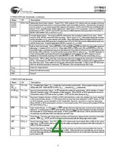
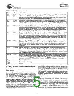
CY7B933 HOTLink Receiver (continued)
Name
INB
I/O
Description
Serial Data Input B. This pin is either a single-ended PECL data receiver (INB) or half of the INB
PECL in
(Diff In)
(INB+)
differential pair. If SO is wired to V , then INB± can be used as differential line receiver interchangeably
CC
with INA±. If SO is normally connected and loaded, INB becomes a single-ended PECL 100K (+5V refer-
enced) serial data input. INB is used as the test clock while in Test mode.
SI
(INB−)
PECL in
(Diff In)
Status Input. This pin is either a single-ended PECL status monitor input (SI) or half of the INB
differential pair. If SO is wired to V , then INB± can be used as differential line receiver interchangeably
CC
with INA±. IfSOisnormallyconnectedandloaded,SIbecomesasingle-endedPECL100K(+5Vreferenced)
status monitor input, which is translated into a TTL-level signal at the SO pin.
SO
RF
TTL Out
TTL In
Status Out. SO is the TTL-translated output of SI. It is typically used to translate the Carrier Detect
output from a fiber-optic receiver connected to SI. When this pin is normally connected and loaded
(without any external pull-up resistor), SO will assume the same logical level as SI and INB will
become a single-ended PECL serial data input. If the status monitor translation is not desired, then
SO may be wired to V and the INB± pair may be used as a differential serial data input.
CC
Reframe Enable. RF controls the Framer logic in the Receiver. When RF is held HIGH, each SYNC
(K28.5) symbol detected in the shifter will frame the data that follows. If is HIGH for 2,048 consecutive
bytes, the internal framer switches to double-byte mode. When RF is held LOW, the reframing logic
is disabled. The incoming data stream is then continuously deserialized and decoded using byte
boundaries set by the internal byte counter. Bit errors in the data stream will not cause alias SYNC
characters to reframe the data erroneously.
REFCLK
MODE
TTL In
Reference Clock. REFCLK is the clock frequency reference for the clock/data synchronizing PLL.
REFCLK sets the approximate center frequency for the internal PLL to track the incoming bit stream.
REFCLK must be connected to a crystal-controlled time base that runs within the frequency limits of
the Tx/Rx pair, and the frequency must be the same as the transmitter CKW frequency (within
CKW±0.1%).
3-Level In Decoder Mode Select. The level on the MODE pin determines the decoding method to be used.
When wired to GND, MODE selects 8B/10B decoding. When wired to V , registered shifter contents
CC
bypass the decoder and are sent to Q directly. When left floating (internal resistors hold the MODE pin at
a−j
V
/2)theinternalbitclockgeneratorisdisabledandINBbecomesthebitratetestclocktobeusedfor factory
CC
test. In typical applications, MODE is wired to V or GND.
CC
BISTEN
TTL In
Built-In Self-Test Enable. When BISTEN is LOW the Receiver awaits a D0.0 (sent once per BIST loop)
character and begins a continuous test sequence that tests the functionality of the Transmitter, the Receiver,
and the link connecting them. In BIST mode the status of the test can be monitored with RDY and RVS
outputs. In normal use BISTEN is held HIGH or wired to V . BISTEN has the same timing as Q
.
CC
0−7
V
V
Power for output drivers.
Power for internal circuitry.
Ground.
CCN
CCQ
GND
In BIST mode, the Input register becomes the signature pat-
tern generator by logically converting the parallel Input register
into a Linear Feedback Shift Register (LFSR). When enabled,
this LFSR will generate a 511-byte sequence that includes all
Data and Special Character codes, including the explicit viola-
tion symbols. This pattern provides a predictable but pseu-
do-random sequence that can be matched to an identical
LFSR in the Receiver.
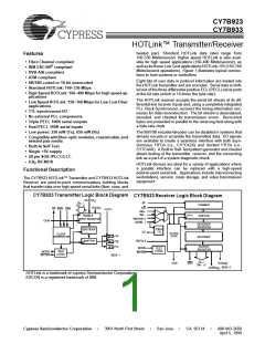
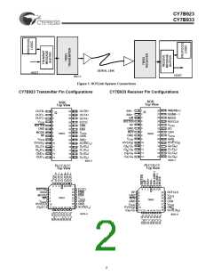
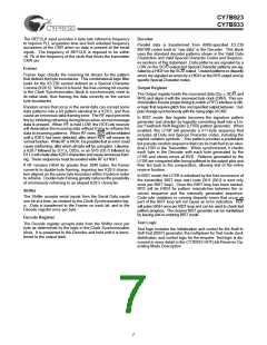
CY7B923 HOTLink Transmitter Block Diagram
Description
Input Register
The Input register holds the data to be processed by the HOT-
Link transmitter and allows the input timing to be made consis-
tent with standard FIFOs. The Input register is clocked by CKW
and loaded with information on the D , SC/D, and SVS pins.
0−7
Two enable inputs (ENA and ENN) allow the user to choose when
data is loaded in the register. Asserting ENA (Enable, active LOW)
causes the inputs to be loaded in the register on the rising edge of
CKW. If ENN (Enable Next, active LOW) is asserted when CKW
rises, the data present on theinputs on the next rising edge of CKW
will be loaded into the Input register. If neither ENA nor ENN are
asserted LOW on the rising edge of CKW, then a SYNC (K28.5)
character is sent. These two inputs allow proper timing and function
for compatibility with either asynchronous FIFOs or clocked FIFOs
without external logic, as shown in Figure 5.
Encoder
The Encoder transforms the input data held by the Input reg-
ister into a form more suitable for transmission on a serial in-
terface link. The code used is specified by ANSI X3.230 (Fibre
Channel) and the IBM ESCON channel (code tables are at the
end of this datasheet). The eight D
data inputs are converted
0−7
to either aData symbol or a Special Character, depending upon the
state of the SC/D input. If SC/D is HIGH, the data inputs represent
a control code and are encoded using the Special Character code
5

 CYPRESS [ CYPRESS ]