CY62187EV30 MoBL®
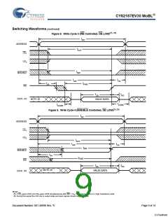
Switching Waveforms (continued)
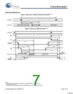
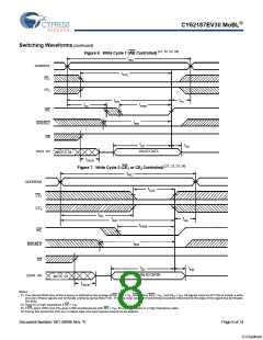
Figure 6. Write Cycle 1 (WE Controlled) [21, 22, 23, 24]
t
WC
ADDRESS
t
SCE
CE
CE
1
2
t
t
HA
AW
t
t
PWE
SA
WE
t
BHE
/
BLE
BW
OE
t
t
SD
HD
VALID DATA
DATA I/O
NOTE 24
t
HZOE
Figure 7. Write Cycle 2 (CE1 or CE2 Controlled) [21, 22, 23, 24]
tWC
ADDRESS
tSCE
CE1
CE2
tSA
tAW
tHA
tPWE
WE
tBW
BHE/BLE
OE
tSD
VALID DATA
tHD
DATA I/O
NOTE 24
tHZOE
Notes
21. The internal Write time of the memory is defined by the overlap of WE, CE = V , BHE and/or BLE = V , and CE = V . All signals must be ACTIVE to initiate a write
1
IL
IL
2
IH
and any of these signals can terminate a write by going INACTIVE. The data input setup and hold timing should be referenced to the edge of the signal that terminates
the write.
22. Data I/O is high impedance if OE = V
.
IH
23. If CE goes HIGH and CE goes LOW simultaneously with WE = V , the output remains in a high impedance state.
1
2
IH
24. During this period the I/Os are in output state and input signals should not be applied.
Document Number: 001-48998 Rev. *E
Page 8 of 14
[+] Feedback

 CYPRESS [ CYPRESS ]