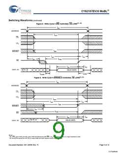
CY62187EV30 MoBL®
DC Input Voltage [3, 4] ..................–0.3 V to VCC (max) + 0.3 V
Output Current into Outputs (LOW) ............................20 mA
Maximum Ratings
Exceeding maximum ratings may impair the useful life of the
device. These user guidelines are not tested.
Static Discharge Voltage......................................... > 2001 V
(per MIL-STD-883, Method 3015)
Storage Temperature ...............................–65 °C to +150 °C
Latch Up Current ....................................................> 200 mA
Ambient Temperature with
Power Applied...........................................–55 °C to +125 °C
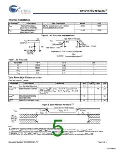
Operating Range
Supply Voltage to Ground
Potential........................................–0.3 V to VCC(max) + 0.3 V
Ambient
Temperature
[5]
Device
Range
VCC
DC Voltage Applied to Outputs
CY62187EV30LL Industrial –40°Cto+85°C 2.2 V to 3.7 V
in High Z State [3, 4].......................–0.3 V to VCC(max) + 0.3 V
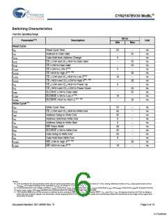
Electrical Characteristics
Over the Operating Range
55 ns
Min Typ[6]
Parameter
VOH
Description
Test Conditions
Unit
Max
Output HIGH Voltage
2.2 V < VCC < 2.7 V
2.7 V < VCC < 3.7 V
2.2 V < VCC < 2.7 V
2.7 V < VCC < 3.7 V
2.2 V < VCC < 2.7 V
2.7 V < VCC < 3.7 V
2.2 V< VCC < 2.7 V
2.7 V < VCC < 3.7 V
GND < VI < VCC
IOH = –0.1 mA
IOH = –1.0 mA
IOL = 0.1 mA
IOL = 2.1 mA
2.0
2.4
–
–
–
–
V
V
–
VOL
VIH
VIL
Output LOW Voltage
Input HIGH Voltage
Input LOW Voltage
–
0.4
V
–
–
0.4
V
1.8
2.2
–0.3
–0.3
–1
–1
–
–
VCC + 0.3 V
V
–
VCC + 0.3 V
V
–
0.6
0.7
+1
+1
55
9
V
–
V
IIX
Input Leakage Current
Output Leakage Current
–
A
A
mA
mA
IOZ
ICC
GND < VO < VCC, Output Disabled
–
VCC Operating Supply
Current
f = fMax = 1/tRC
f = 1 MHz
VCC = VCC(max)
OUT = 0 mA
CMOS levels
45
7.5
I
–
[7]
ISB2
Automatic CE
Power Down
CE1 > VCC – 0.2 V or CE2 < 0.2 V or
(BHE and BLE) > VCC – 0.2 V,
–
8
48
A
Current—CMOS Inputs
V
V
IN > VCC – 0.2 V or VIN < 0.2 V, f = 0,
CC = 3.7 V
Capacitance
Parameter[8]
Description
Test Conditions
Max
Unit
CIN
Input Capacitance
TA = 25 °C, f = 1 MHz, VCC = VCC(typ)
25
35
pF
pF
COUT
Output Capacitance
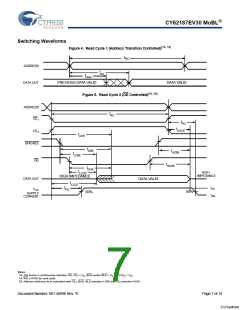
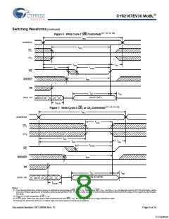
Notes
3.
4.
V
V
= –2.0V for pulse durations less than 20 ns.
IL(min)
= V + 0.75V for pulse durations less than 20 ns.
IH(max)
CC
5. Full Device AC operation assumes a 100 s ramp time from 0 to V (min) and 200 s wait time after V stabilization.
CC
CC
6. Typical values are included for reference only and are not guaranteed or tested. Typical values are measured at V = V
, T = 25 °C.
A
CC
CC(typ)
7. Chip enables (CE and CE ) and Byte enables (BHE and BLE) need to be tied to CMOS levels to meet the I
/ I
spec. Other inputs can be left floating.
1
2
SB2 CCDR
8. Tested initially and after any design or process changes that may affect these parameters.
Document Number: 001-48998 Rev. *E
Page 4 of 14
[+] Feedback

 CYPRESS [ CYPRESS ]