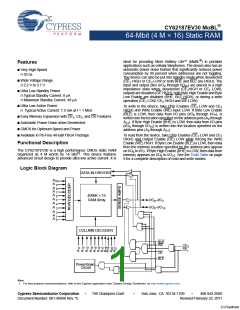
CY62187EV30 MoBL®
Thermal Resistance
Parameter[9]
Description
Test Conditions
FBGA
Unit
JA
Thermal Resistance
(Junction to Ambient)
Still Air, soldered on a 3 × 4.5 inch,
2-layer printed circuit board
59.06
C/W
JC
Thermal Resistance
(Junction to Case)
14.08
C/W
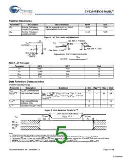
Figure 2. AC Test Loads and Waveforms
ALL INPUT PULSES
90%
10%
R1
VCC
OUTPUT
VCC
90%
10%
GND
Fall Time = 1 V/ns
R2
30 pF
Rise Time = 1 V/ns
INCLUDING
JIG AND
SCOPE
Equivalent to: THEVENIN EQUIVALENT
RTH
OUTPUT
V
Table 1. AC Test Loads
Parameter
R1
2.5 V
16667
15385
8000
3.3 V
Unit
1103
1554
645
R2
RTH
VTH
1.20
1.75
V
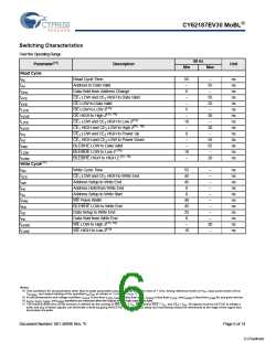
Data Retention Characteristics
Over the Operating Range
Parameter
Description
Conditions
Min
1.5
–
Typ[10]
Max
–
Unit
V
VDR
VCC for Data Retention
–
–
[11]
ICCDR
Data Retention Current VCC = 1.5 V, CE1 > VCC – 0.2 V or CE2 < 0.2 V or
(BHE and BLE) > VCC – 0.2 V, VIN > VCC – 0.2 V or
48
A
VIN < 0.2 V
[9]
tCDR
Chip Deselect to Data
Retention Time
0
–
–
–
–
ns
ns
[12]
tR
Operation Recovery Time
55
Figure 3. Data Retention Waveform [13]
DATA RETENTION MODE
> 1.5 V
VCC(min)
tCDR
VCC(min)
tR
VDR
VCC
CE or
1
BHE.BLE
or
CE
2
Notes
9. Tested initially and after any design or process changes that may affect these parameters.
10. Typical values are included for reference only and are not guaranteed or tested. Typical values are measured at V = V
, T = 25 °C.
CC
CC(typ)
A
11. Chip enables (CE and CE ) and Byte enables (BHE and BLE) need to be tied to CMOS levels to meet the I
/ I
spec. Other inputs can be left floating.
1
2
SB2 CCDR
12. Full device operation requires linear V ramp from V to V
13. BHE.BLE is the AND of both BHE and BLE. Chip is deselected by either disabling the chip enable signals or by disabling both BHE and BLE.
> 100 s or stable at V
> 100 s.
CC
DR
CC(min)
CC(min)
Document Number: 001-48998 Rev. *E
Page 5 of 14
[+] Feedback

 CYPRESS [ CYPRESS ]