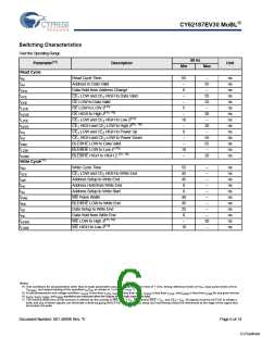
CY62187EV30 MoBL®
Switching Characteristics
Over the Operating Range
55 ns
Unit
Parameter[14]
Description
Min
Max
Read Cycle
tRC
Read Cycle Time
Address to Data Valid
55
–
–
55
–
ns
ns
ns
ns
ns
ns
ns
ns
ns
ns
ns
ns
ns
ns
tAA
tOHA
tACE
tDOE
tLZOE
tHZOE
tLZCE
tHZCE
tPU
Data Hold from Address Change
CE1 LOW and CE2 HIGH to Data Valid
OE LOW to Data Valid
OE LOW to LOW Z[15]
OE HIGH to High Z[15, 16]
CE1 LOW and CE2 HIGH to Low Z[15]
CE1 HIGH and CE2 LOW to High Z[15, 16]
CE1 LOW and CE2 HIGH to Power Up
CE1 HIGH and CE2 LOW to Power Down
BLE/BHE LOW to Data Valid
6
–
55
25
–
–
5
–
20
–
10
–
20
–
0
tPD
–
55
55
–
tDBE
tLZBE
tHZBE
Write Cycle[17]
tWC
–
BLE/BHE LOW to Low Z [15]
BLE/BHE HIGH to HIGH Z [15, 16]
10
–
20
Write Cycle Time
55
45
45
0
–
–
ns
ns
ns
ns
ns
ns
ns
ns
ns
ns
ns
tSCE
tAW
CE1 LOW and CE2 HIGH to Write End
Address Setup to Write End
Address Hold from Write End
Address Setup to Write Start
WE Pulse Width
–
tHA
–
tSA
0
–
tPWE
tBW
40
45
25
0
–
BLE/BHE LOW to Write End
Data Setup to Write End
Data Hold from Write End
WE LOW to High Z[15, 16]
WE HIGH to Low Z[15]
–
tSD
–
tHD
–
tHZWE
tLZWE
–
20
–
10
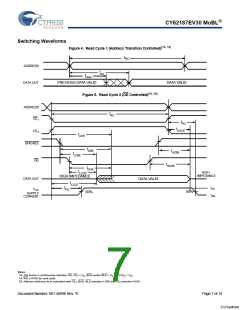
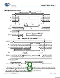
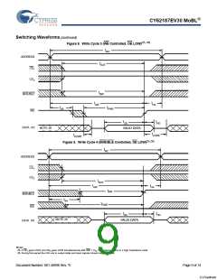
Notes
14. Test conditions for all parameters other than tri-state parameters assume signal transition time of 1 V/ns, timing reference levels of V , input pulse levels of 0 to
TH
V
, and output loading of the specified I /I as shown in Table 1 on page 5.
CC(typ)
OL OH
15. At any temperature and voltage condition, t
is less than t
, t
is less than t
, t
is less than t
, and t
is less than t
for any given device.
LZWE
HZCE
LZCE HZBE
LZBE HZOE
LZOE
HZWE
16. t
, t
, t
, and t
transitions are measured when the outputs enter a high impedence state.
HZOE HZCE HZBE
HZWE
17. The internal Write time of the memory is defined by the overlap of WE, CE = V , BHE and/or BLE = V , and CE = V . All signals must be ACTIVE to initiate a
1
IL
IL
2
IH
write and any of these signals can terminate a write by going INACTIVE. The data input setup and hold timing should be referenced to the edge of the signal that
terminates the write.
Document Number: 001-48998 Rev. *E
Page 6 of 14
[+] Feedback

 CYPRESS [ CYPRESS ]