BCM4330 Preliminary Data Sheet
Signal Assignments
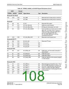
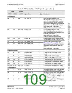
Table 18: FCFBGA, WLBGA, and WLCSP Signal Descriptions (Cont.)
Bump#
WLCSP Signal Name
Ball#
FCFBGA WLBGA
Miscellaneous
Type Description
L9
L9
106
WL_REG_ON
I
Used by PMU (OR-gated with
BT_REG_ON) to power up or power
down the internal BCM4330 regulators
used by the WLAN section. This pin is
also a low-asserting reset for WLAN only
(Bluetooth is not affected by this pin).
Logic High Level: 1.08V–3.6V
200k pull-down resistor included.
K9
K10
G10
107–108 BT_REG_ON
I
I
Used by PMU (OR-gated with
WL_REG_ON) to power up or power
down internal BCM4330 regulatorsused
by the BT/FM section.
Logic High Level: 1.08V–3.6V
200k pull-down resistor included.
F10
131
BT_RST_N
Low asserting reset for Bluetooth/FM
only (WLAN is not affected by this pin).
J9
J10
K9
J10
111–112 EXT_SMPS_REQ
109–110 EXT_PWM_REQ
I
I
Auxiliary PMU control inputs (see
“Reset Circuits” on page 31). These pins
have 200k internal pull-down resistors
and should be no-connect when not
used.
Logic High Level: 1.08V–3.6V
Bluetooth Supplies
A7
A8
68
BT_PAVDD3P3
I
3.3V Bluetooth internal PA power
supply
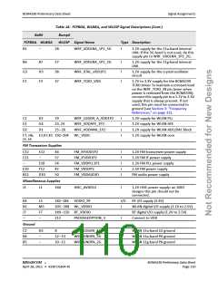
–
B9
–
A11
B8
B11
–
BT_RFVDD1P2
BT_LNAVDD1P2
BT_VCOVDD1P2
BT_IFVDD1P2
I
I
I
I
I
I
1.2V Bluetooth power supply
A9
A10
B7
67
64
59
61
1.2V Bluetooth LNA power supply
1.2V Bluetooth VCO power supply
1.2V Bluetooth IF block power supply
1.2V Bluetooth PLL power supply
1.2V Bluetooth baseband core supply
B10
BT_PLLVDD1P2
F8, J8, K8 K8, E8
138–148 BT_VDDC
WLAN Supplies
A3
A4
–
–
33, 34
31, 32
–
WRF_VDDPA_5G
I
I
I
I
VDD power supply (from VBAT) for the
internal 11a-band power amplifier
VDD power supply (from VBAT) for the
internal 11g-band power amplifier
VDD power supply (from VBAT) for both
internal power amplifiers
VDD power supply (from VBAT) supply
for the WLAN PA driver
–
WRF_VDDPA_2G
WRF_VDDPA
A4
C3
C4
30
WRF_PADRV_VDD
®
BROADCOM
BCM4330 Preliminary Data Sheet
April 28, 2011 • 4330-DS304-RI
Page 109

 CYPRESS [ CYPRESS ]