BCM4330 Preliminary Data Sheet
Signal Assignments
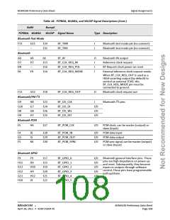
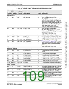
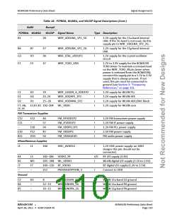
Table 18: FCFBGA, WLBGA, and WLCSP Signal Descriptions (Cont.)
Bump#
WLCSP Signal Name
213–225 WL_VSS
Ball#
FCFBGA WLBGA
Type Description
WLAN ground
–
–
I
No Connect
A1, A2
K7
–
–
–
181
NC
N/A No connect
No connect
VDD_ISLAND
I
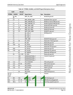
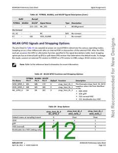
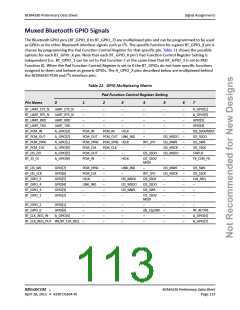
WLAN GPIO Signals and Strapping Options
The pins listed in Table 19 are sampled at power-on reset (POR) to determine the various operating modes.
Sampling occurs a few milliseconds after an internal POR or deassertion of the external POR. After the POR,
each pin assumes the GPIO or alternative function specified in the signal descriptions table. Each strapping
option pin has an internal pull-up (PU) or pull-down (PD) resistor that determines the default mode. To change
the mode, connect an external PU resistor to VDDIO or a PD resistor to GND, using a 10 kΩ resistor or less.
Note: Refer to the reference board schematics for more information.
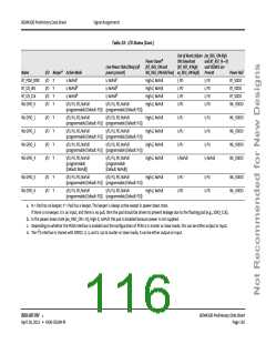
Table 19: WLAN GPIO Functions and Strapping Options
FCFBGA WLBGA WLCSP
Pin Name
Pin #
Pin #
Pin #
Default Function
Description
SDIO_DATA_1 M5
SDIO_DATA_2 M8
M8
M5
D8
179
180
181
X
X
0
strap_host_ifc_1 Thethreepinsstrap_host_ifc_[3:1]
together select the host interface
strap_host_ifc_2
mode:
WL_GPIO_6
H4
strap_host_ifc_3
• 0XX: SDIO
• 10X: gSPI
• 110: normal HSIC
• 111: bootloader-less HSIC
Table 20: Strap Options
strap_host_ifc_2
SDIO_DATA_2
strap_host_ifc_1
SDIO_DATA_1
strap_host_ifc_3
WL_GPIO_6
Default states at sampling instant
SDIO
gSPI
HSIC (normal)
0
0
1
1
1
Float
Float
x
x
0
1
x
0
1
1
Bootloader-less HSIC (debug only)
®
BROADCOM
BCM4330 Preliminary Data Sheet
April 28, 2011 • 4330-DS304-RI
Page 112

 CYPRESS [ CYPRESS ]