BCM4330 Preliminary Data Sheet
Signal Assignments
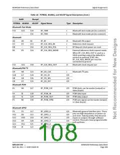
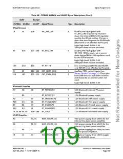
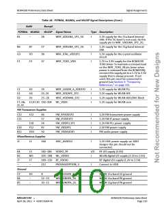
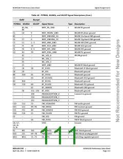
Table 18: FCFBGA, WLBGA, and WLCSP Signal Descriptions (Cont.)
Bump#
WLCSP Signal Name
Ball#
FCFBGA WLBGA
Bluetooth Test Mode
Type Description
F11
–
G11
–
133
132
BT_TM0
BT_TM1
I
I
Bluetooth test mode pin (no connect)
Bluetooth test mode pin (no connect)
Bluetooth
A8
D7
D8
E8
A9
D7
–
66
BT_RF
O
I
I
Bluetooth PA output
Reference clock request
BT Request clock power on reset
External reference clock request mode.
113
116
114
BT_CLK_REQ_IN
BT_CLK_REQ_POL
BT_CLK_REQ_MODE
E9
I
When BT_CLK_REQ_OUT is used as a
HIGH asserting output (by default) to
control an external TCXO, this
BT_CLK_REQ_MODE pin must be
connected to ground.
F12
G12
118
BT_CLK_REQ_OUT
O
Bluetooth clock request out
Bluetooth/FM I2S
2
G9
G10
H8
H8
G7
G8
H7
123
124
126
125
BT_I2S_CLK
BT_I2S_DI
BT_I2S_WS
BT_I2S_DO
I
Bluetooth I S pins
I/O
I/O
I/O
H9
Bluetooth PCM
E5
H6
127
BT_PCM_CLK
I/O
PCM clock, can be master (output) or
slave (input)
F4
G5
F5
J6
J5
K6
128
129
130
BT_PCM_IN
BT_PCM_OUT
BT_PCM_SYNC
I/O
I/O
I/O
PCM data input
PCM data output
PCM sync signal, can be master (output)
or slave (input)
Bluetooth GPIO
F9
F9
117
115
119
120
121
122
BT_GPIO_0
BT_GPIO_1
BT_GPIO_2
BT_GPIO_3
BT_GPIO_4
BT_GPIO_5
I/O
I/O
I/O
I/O
I/O
I/O
Bluetooth general interface pins. These
pins are high-impedance on power up
and reset. Subsequently, they become
inputs or outputs through software
control. These pins have programmable
pull-up/down.
H11
G12
H12
G11
H10
D9
H10
H9
H12
J9
®
BROADCOM
BCM4330 Preliminary Data Sheet
April 28, 2011 • 4330-DS304-RI
Page 108

 CYPRESS [ CYPRESS ]