BCM4330 Preliminary Data Sheet
Signal Assignments
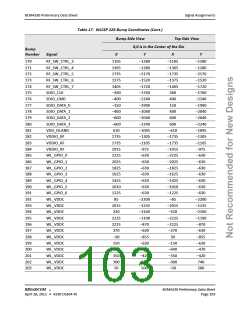
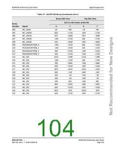
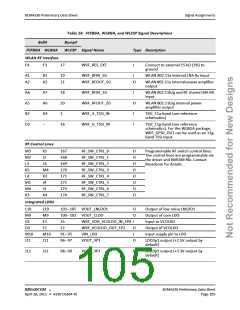
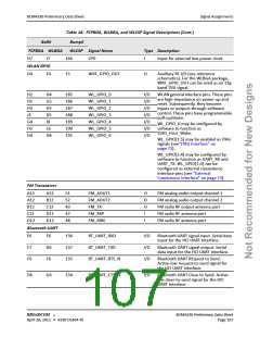
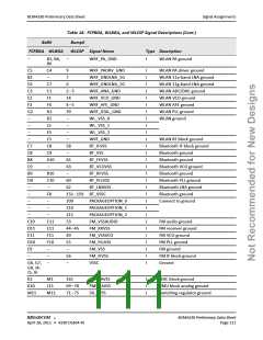
Table 18: FCFBGA, WLBGA, and WLCSP Signal Descriptions (Cont.)
Bump#
WLCSP Signal Name
Ball#
FCFBGA WLBGA
Type Description
H7
J7
166
LPO
I
Input for external low-power clock
WLAN GPIO
D4
E4
15
WRF_GPIO_OUT
O
Auxiliary RF I/O (see reference
schematics). For the WLBGA package,
WRF_GPIO_OUT can be used as an 11g-
band TSSI signal.
H2
H1
H3
J3
G4
H5
H4
H4
G5
H5
D5
J8
185
186
187
188
189
190
191
WL_GPIO_0
WL_GPIO_1
WL_GPIO_2
WL_GPIO_3
WL_GPIO_4
WL_GPIO_5
WL_GPIO_6
I/O
I/O
I/O
I/O
I/O
I/O
I/O
WLAN general interface pins. These pins
are high-impedance on power up and
reset. Subsequently, they become
inputs or outputs through software
control. These pins have programmable
pull-up/down.
WL_GPIO_0 may be configured by
software to function as
SDIO_Host_Wake.
L6
D8
WL_GPIO[1:5] may be enabled as JTAG
signals (see“JTAG Interface” on
page 73).
WL_GPIO[3:4] may be configured by
software to function as UART_RX and
UART_TX. WL_GPIO[1:5] can be
configured as external coexistence
interface pins (see “External
Coexistence Interface” on page 73).
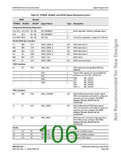
FM Transceiver
A11
A12
B12
E12
D12
A12
B12
C12
D11
D12
51
52
43
47
48
FM_AOUT1
FM_AOUT2
FM_TX
FM_RXP
FM_RXN
O
O
O
I
FM analog audio output channel 1
FM analog audio output channel 2
FM radio RF output antenna port
FM radio RF antenna port
I
FM radio RF antenna port
Bluetooth UART
E6
E7
F6
E6
D6
F6
136
137
135
BT_UART_RXD
BT_UART_TXD
BT_UART_RTS_N
I/O
I/O
I/O
Bluetooth UART signal input. Serial data
input for the HCI UART Interface.
Bluetooth UART signal output. Serial
data input for the HCI UART Interface.
Bluetooth UART REquest to Send.
Active-low request-to-send signal for
the HCI UART interface.
D6
G6
134
BT_UART_CTS_N
I/O
Bluetooth UART Clear to Send. Active-
low clear-to-send signal for the HCI
UART interface.
®
BROADCOM
BCM4330 Preliminary Data Sheet
April 28, 2011 • 4330-DS304-RI
Page 107

 CYPRESS [ CYPRESS ]