Application Information ......
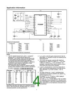
FREQUENCY
MODULATOR
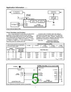
Rx FREQUENCY
DISCRIMINATOR
SIGNAL AND
DC LEVEL
ADJUSTMENT
SIGNAL AND
DC LEVEL
ADJUSTMENT
Rx SIGNAL IN
Rx FEEDBACK
Tx OUT
Rx
Tx
CIRCUITS
CIRCUITS
RxD
RxC
TxD
TxC
Rx DATA
Rx CLOCK
Tx DATA
µCONTROLLER
FX589
GMSK MODEM
or UART
Tx CLOCK
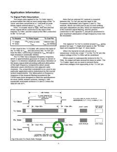
Fig.3 External Signal Paths
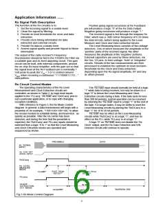
Clock Oscillator and Dividers
The Tx and (nominal) Rx data rates are determined
by division of the frequency present at the Xtal pin,
which may be generated by the on-chip Xtal oscillator
or be derived from an external source. Any Xtal/clock
frequency in the range 1.0MHz to 5.0MHz (VDD = 3.0V)
or 1.0MHz to 8.2MHz (VDD = 5.0V) may be employed,
depending upon the desired data rate.
A division ratio to facilitate data-rate setting is
controlled by the logic level inputs on the ClkDivA/B
pins, and is shown in Table 1 (below) - together with
examples of how various ‘standard’ data-rates may be
derived from common µP or Xtal frequencies.
Data Rate =
Xtal/Clock Frequency
Division Ratio (ClkDivA/B)
Xtal/Clock Frequency (MHz)
Notethe device operation is not guaranteed
above 64,000 bits/s or below 4,000 bits/s at
the relevant supply voltage
8.192
4.9152
4.096
[12.288/3]
2.4576
[12.288/5]
2.048
[6.144/3]
Inputs
ClkDiv ClkDiv
Division Ratio:
Xtal Freq
Data Rate (b/s)
A
0
0
1
1
B
0
1
0
1
Data Rate
128
64000*
32000
16000
8000
38400*
19200
9600
32000
16000
8000
19200
9600
4800
16000
8000
4000
256
512
1024
4800
4000
Table 1 Clock/Data Rates
* VDD >= 4.5V
Fig.4 Minimum µController System Connections
5

 CMLMICRO [ CML MICROCIRCUITS ]