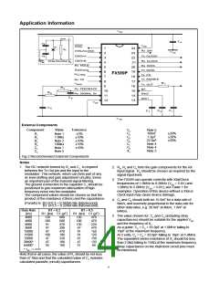
Application Information
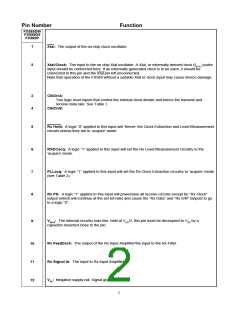
VDD
XTAL
1
C 4
C
3
VDD
XTAL
X
1
1
24
23
22
21
20
19
18
17
16
15
14
13
R
2
Rx S/N
XTAL/CLOCK
V SS
2
C
2
ClkDivA
ClkDivB
Rx HOLD
RxDCacq
PLLacq
Tx CLOCK
Rx CLOCK
Rx DATA
Tx DATA
3
2
XTAL/CLOCK
V
SS
4
5
6
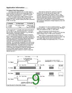
FX589P
Tx PS
7
Tx ENABLE
Rx PS
VBIAS
8
R 1
Tx OUT
9
R 4
Rx FEEDBACK
Rx SIGNAL IN
BT
10
11
12
R 3
Doc2
C 6
Doc1
VSS
C 5
C 8
C 1
C 7
V SS
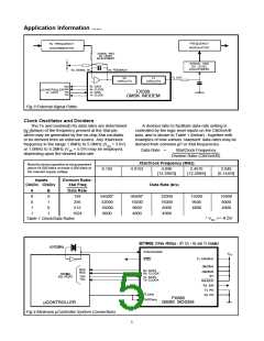
External Components
Component
Value
Tolerance
±5%
C3
Note 5
100nF
1.0µF
22.0pF
Note 4
Note 4
Note 3
C4
C5
C6
C7
C8
X1
±20%
±20%
±20%
R1
R2
R3
R4
C1
C2
Note 1
1.0MΩ
Note 2
100kΩ
Note 1
Note 5
±10%
±10%
±10%
±10%
Fig.2 Recommended External Components
Notes
1. The RC network formed by R1 and C1 is required
between the Tx Out pin and the input to the
2. R3, R4 and C6 form the gain components for the Rx
Input signal. R3 should be chosen as required by the
signal input level.
modulator. This network, which can form part of any
dc level shifting and gain adjustment circuitry, forms
an important part of the transmit signal filtering.
The ground connection to the capacitor C should be
positioned to give maximum attenuation o1f high-
frequency noise into the modulator.
3. The FX589 can operate correctly with Xtal/Clock
frequencies of 1.0MHz to 8.2MHz (VDD = 5.0V) and
1.0MHz to 5.0MHz (VDD = 3.0V); see Table 1 for
examples. Operation of this device without a Xtal or
Clock input may cause device damage.
The component values should be chosen so that the
product of the resistance (Ohms) and the capacitance
4. C7 and C8 should both be 15.0nF for a data rate of
8kb/s, and inversely proportional to the data rate for
other data rates, e.g. 30.0nF at 4kb/s, 1.8nF at
64kb/s.
(Farads) is: BT of 0.3 = 0.34/bit rate (bits/second)
BT of 0.5 = 0.22/bit rate (bits/second).
Data Rate
(b/s)
BT = 0.3
R1 (kΩ) C1 (pF)
BT = 0.5
R1 (kΩ) C1 (pF)
5. The value chosen for C2 and C3 (including stray
capacitances) should be suitable for the applied VDD
and the frequency of X1.
4000
4800
8000
9600
16000
19200
32000
38400*
64000*
* VDD >= 4.5V
120
100
91
91
47
100
47
47
680
680
470
390
470
180
220
180
100
120
100
120
47
91
91
47
47
51
470
470
220
470
150
120
150
120
68
As a guide: C2 = C3 = 33.0pF at 1.0MHz falling to
18pF at the maximum frequency.
At 3 volts, C2 = C3 = 33.0pF falling to 18pF at 5.0MHz.
The equivalent series resistance of X1 should be less
than 2.0kΩ falling to 150Ω at the maximum frequency.
Stray capacitance on the Xtal/clock circuit pins must
be minimised.
56
Note that in all cases, the value of R1 should be not less
than 47.0kΩ and that the calculated value of C1 includes
calculated parasitic (circuit) capacitances.
4

 CMLMICRO [ CML MICROCIRCUITS ]