Pin Number
Function
FX589DW
FX589D5
FX589P
13
14
Doc1:
Doc2:
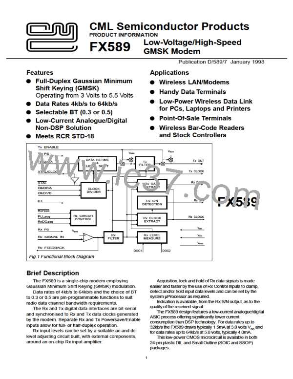
Connections to the Rx Level Measurement Circuitry. A capacitor should be connected
from each pin to VSS. See Figure 2.
15
BT: A logic level to select the modem ‘BT’ (the ratio of the Tx Filter's -3dB frequency to the Bit-
Rate). A logic “1” sets the modem to a BT of 0.5, a logic “0” to a BT of 0.3.
16
17
Tx Out: The Tx signal output from the FX589 GMSK Modem.
Tx Enable: A logic “1” applied to this input enables the transmit data path through the Tx Filter to
the “Tx Out” pin. A logic “0” will put the “Tx Out” pin to VBIAS via a high impedance.
18
19
Tx PS: A logic “1” applied to this input will powersave all transmit circuits except for the “Tx
Clock”.
Tx Data: The logic level input for the data to be transmitted. This data should be synchronous
with the “Tx Clock”.
20
21
22
Rx Data: A logic level output carrying the received data, synchronous with the “Rx Clock”.
Rx Clock: A logic level clock output at the received data bit-rate.
Tx Clock: A logic level clock output at the transmit-data rate.
23
24
Rx S/N: A logic level output which may be used as an indication of the quality of the received
signal.
VDD: Positive supply rail. A single, stable power supply is required. Levels and voltages within this
modem are dependent upon this supply. This pin should be decoupled to VSS by a capacitor
mounted close to the pin.
3

 CMLMICRO [ CML MICROCIRCUITS ]