Pin Number
Function
FX589DW
FX589D5
FX589P
1
2
Xtal: The output of the on-chip clock oscillator.
Xtal/Clock: The input to the on-chip Xtal oscillator. A Xtal, or externally derived clock (fXTAL) pulse
input should be connected here. If an externally generated clock is to be used, it should be
connected to this pin and the Xtal pin left unconnected.
Note that operation of the FX589 without a suitable Xtal or clock input may cause device damage.
3
4
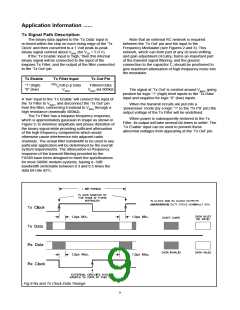
ClkDivA:
Two logic level inputs that control the internal clock divider and hence the transmit and
receive data rate. See Table 1.
ClkDivB:
5
6
7
8
Rx Hold: A logic “0” applied to this input will ‘freeze’ the Clock Extraction and Level Measurement
circuits unless they are in ‘acquire’ mode.
RXDCacq: A logic “1” applied to this input will set the Rx Level Measurement circuitry to the
‘acquire’ mode.
PLLacq: A logic “1” applied to this input will set the Rx Clock Extraction circuitry to ‘acquire’ mode
(see Table 2).
Rx PS: A logic “1” applied to this input will powersave all receive circuits except for “Rx Clock”
output (which will continue at the set bit-rate) and cause the “Rx Data” and “Rx S/N” outputs to go
to a logic “0”.
V
BIAS: The internal circuitry bias line, held at VDD/2, this pin must be decoupled to VSS by a
9
capacitor mounted close to the pin.
Rx Feedback: The output of the Rx Input Amplifier/the input to the Rx Filter.
Rx Signal In: The input to Rx Input Amplifier.
10
11
12
VSS: Negative supply rail. Signal ground.
2

 CMLMICRO [ CML MICROCIRCUITS ]