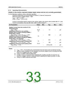
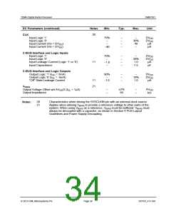
TDMA Digital Radio Processor
CMX7161
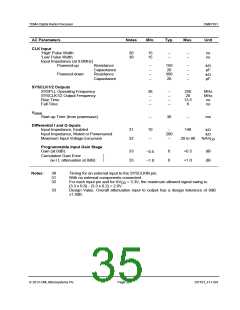
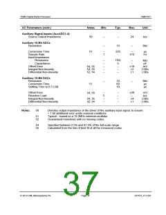
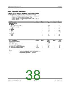
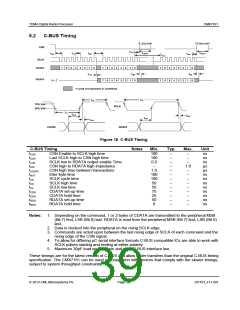
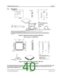
AC Parameters
Notes
Min.
Typ.
Max.
Unit
Modulator Outputs
Power-up to Output Stable
Output Coarse Gain Attenuators
Attenuation (at 0dB)
40
–
50
0
100
µs
42
42
+0.2
dB
0.2
Cumulative Attenuation Error
(w.r.t. attenuation at 0dB)
Output Impedance
0
600
TBD
+0.6
–
–
dB
k
0.6
–
–
41
41
Enabled
Disabled
Output Voltage Range
Load Resistance
43, 44
0.3
20
–
–
AV
V
DD-0.3
–
k
40
Power-up refers to issuing a C-BUS command to turn on an output. These limits
apply only if V is on and stable. At power supply switch-on, the default state is
Notes:
BIAS
for all blocks, except the C-BUS interface, to be in placed in powersave mode.
41
42
Small signal impedance, at AV = 3.3V and TAMB = 25°C.
Figures relate to attenuator block only. Design Value. Overall attenuation input to
output has a design tolerance of 0dB ±1.0dB.
DD
43
44
For each output pin. With respect to the output driving a 20k load to AV /2.
The levels of the MOD2/1 Output Fine Gain and Offsets (registers $5D and $5E)
should be adjusted so that the output voltage remains between 20% and 80% of
DD
AV
on each output pin (when 0dB of coarse output gain is used). This will
DD
produce the best performance when the device operates with AV = 3.3V.
DD
2013 CML Microsystems Plc
Page 36
D/7161_FI-1.0/4

 CMLMICRO [ CML MICROCIRCUITS ]