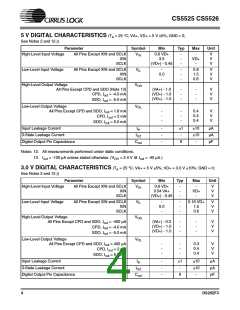
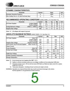
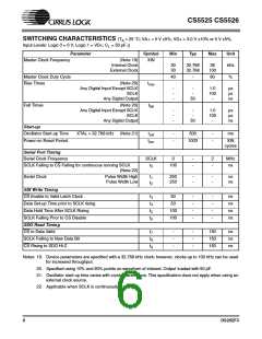
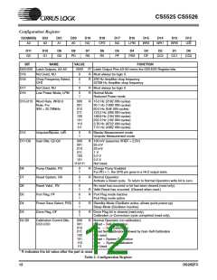
CS5525 CS5526
spect to ground, making the converters ideal for
thermocouple temperature measurements.
DETAILED DESCRIPTION
The CS5525 and CS5526 are 16-bit and 20-bit pin
compatible converters which include a chopper-
stabilized instrumentation amplifier input, and an
on-chip programmable gain amplifier. They are
both optimized for measuring low-level unipolar or
bipolar signals in process control and medical ap-
plications.
Theory of Operation
The CS5525/26 A/D converters are designed to op-
erate from a single +5 V analog supply and provide
several different input ranges. See the Analog
Characteristics section on page 3 for details.
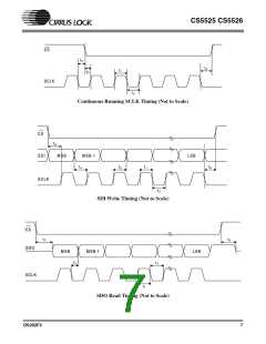
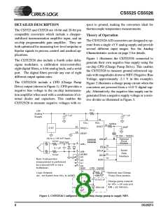
Figure 1 illustrates the CS5525/26 connected to
generate their own negative bias supply using the
on-chip CPD (Charge Pump Drive). This enables
the CS5525/26 to measure ground referenced sig-
nals with magnitudes down to NBV (Negative Bias
Voltage, approximately -2.1 V in this example).
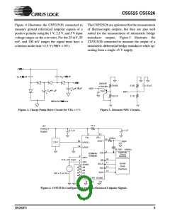
Figure 2 illustrates a charge pump circuit when the
converters are powered from a +3.0 V digital sup-
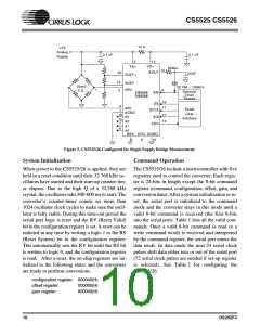
ply. Alternatively, the negative bias supply can be
generated from a negative supply voltage or a resis-
tive divider as illustrated in Figure 3.
The CS5525/26 also include a fourth order delta-
sigma modulator, a calibration microcontroller,
eight digital filters, a 4-bit analog latch, and a serial
port. The digital filters provide any one of eight
different output update rates.
The CS5525/26 include a CPD (Charge Pump
Drive) output (shown in Figure 1). CPD provides a
negative bias voltage to the on-chip instrumenta-
tion amplifier when used with a combination of ex-
ternal diodes and capacitors. This enables the
CS5525/26 to measure negative voltages with re-
Ω
10
+5V
Analog
µ
µ
F
0.1
F
0.1
S upply
2
13
VD+
V A+
500kΩ
10
9
XOUT
20
19
p
20
F
2.5V
VRE F+
VREF-
32.768 ~ 100kH z
Optional
U p to
100 m V Input
XIN
C S5525
C S5526
Ω
10 k
Clock
BAV199
3
Source
AIN +
18
CS
µ
0.1
F
11
4
1
16
S erial
Data
SCLK
AIN-
AGND
A3
17
14
Ω
10 k
SDI
Interface
15
7
Note: Cold-junction
SDO
A2
A1
measurem ent is perform ed
by a second A /D or via a
multiplexer.
6
A0
NBV
CPD DGND
5
8
12
Logic O utputs:
* Optional, see Charge
Ω
5M
A 0 - A 3 S witch from VA + to A GND .
*
Pump Drive section.
µ
0.015
F
C harge-pump network
for V D+ = 5V only and
XIN = 32.768 kH z.
1N4148
µ
1N4148
10
F
+
Figure 1. CS5525/26 Configured to use on-chip charge pump to supply NBV.
8
DS202F3

 CIRRUS [ CIRRUS LOGIC ]