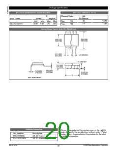
Application Information: continued
For most PCBs the copper thickness, t, is 35µm (1.37 mils)
for one ounce copper; ρ = 717.86µΩ-mil.
Thermal Management
For a CPU load of 16A the resistance needed to create a
50mV drop at full load is:
Thermal Considerations for Power MOSFETs
In order to maintain good reliability, the junction tempera-
ture of the semiconductor components should be kept to a
maximum of 150°C or lower. The thermal impedance
(junction to ambient) required to meet this requirement
can be calculated as follows:
50mV
IOUT
50mV
16A
RDROOP
=
=
= 3.1mΩ.
The resistivity of the copper will drift with the temperature
according to the following guidelines:
TJ(MAX) - TA
Thermal Impedance =
Power
∆R = 12% @ TA = +50˚C;
∆R = 34% @TA = +100˚C.
A heatsink may be added to TO-220 components to reduce
their thermal impedance. A number of PC board layout
techniques such as thermal vias and additional copper foil
area can be used to improve the power handling capability
of surface mount components.
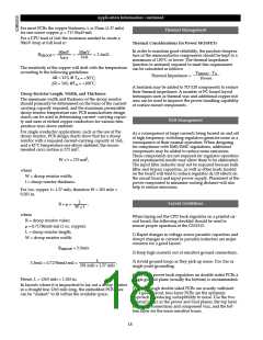
Droop Resistor Length, Width, and Thickness
The minimum width and thickness of the droop resistor
should primarily be determined on the basis of the current-
carrying capacity required, and the maximum permissible
droop resistor temperature rise. PCB manufacturer design
charts can be used in determining current- carrying capaci-
ty and sizes of etched copper conductors for various tem-
perature rises above ambient.
EMI Management
For single conductor applications, such as the use of the
droop resistor, PCB design charts show that for a droop
resistor with a required current-carrying capacity of 16A,
and a 45˚C temperature rise above ambient, the recom-
mended cross section is 275 mil2.
As a consequence of large currents being turned on and off
at high frequency, switching regulators generate noise as a
consequence of their normal operation. When designing
for compliance with EMI/EMC regulations, additional
components may be added to reduce noise emissions.
These components are not required for regulator operation
and experimental results may allow them to be eliminated.
The input filter inductor may not be required because bulk
filter and bypass capacitors, as well as other loads located
on the board will tend to reduce regulator di/dt effects on
the circuit board and input power supply. Placement of the
power component to minimize routing distance will also
help to reduce emissions.
W × t = 275 mil2,
where
W = droop resistor width;
t = droop resistor thickness.
For 1oz. copper, t= 1.37 mils, therefore W = 201 mils =
0.201 in.
L
W × t
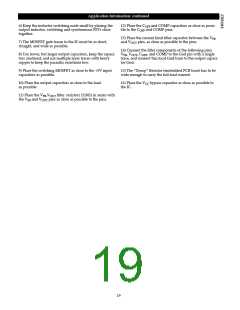
Layout Guidelines
R = ρ ×
,
where
R = droop resistor value;
When laying out the CPU buck regulator on a printed cir-
cuit board, the following checklist should be used to
ensure proper operation of the CS51313.
ρ = 0.71786mΩ-mil (1 oz. copper);
L = droop resistor length;
W = droop resistor width.
1) Rapid changes in voltage across parasitic capacitors and
abrupt changes in current in parasitic inductors are major
concerns for a good layout.
RDROOP = 3.3mΩ.
2) Keep high currents out of sensitive ground connections.
L
3) Avoid ground loops as they pick up noise. Use star or
single point grounding.
3.3mΩ = 0.71786mΩ-mil ×
.
201 mils × 1.37 mils
4) For high power buck regulators on double-sided PCBs a
single ground plane (usually the bottom) is recommended.
Hence, L = 1265 mils = 1.265 in.
In layouts where it is impractical to lay out a droop resistor
in a straight line 1265 mils long, the embedded PCB trace
can be “snaked” to fit within the available space.
5) Even though double sided PCBs are usually sufficient
for a good layout, four-layer PCBs are the optimum
approach to reducing susceptibility to noise. Use the two
internal layers as the power and Gnd planes, the top layer
for power connections and component vias, and the bot-
tom layer for the noise sensitive traces.
18

 CHERRY [ CHERRY SEMICONDUCTOR CORPORATION ]